 | ÐлекÑÑоннÑй компоненÑ: IRIS4011 | СкаÑаÑÑ:  PDF PDF  ZIP ZIP |
Äîêóìåíòàöèÿ è îïèñàíèÿ www.docs.chipfind.ru
Data SheetNo. PD60188-B
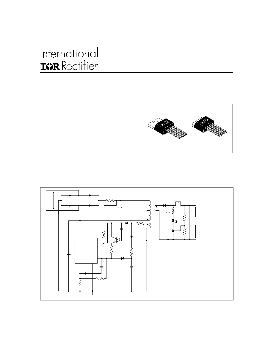
Typical Connection Diagram
INTEGRATED SWITCHER
Description
The IRIS4011(K) is a dual mode voltage and current controller combined with a MOSFET in a single package.
The IRIS4011(K) is designed for use in universal and single input AC/DC and DC/DC switching power supplies
and is capable of powers up to 60W for a universal line input. The device can operate in either a quasi-resonant or
Pulse Ratio Control (PRC) mode, and thereby variable frequency operation.
www.irf.com
1
Features
·
Primary current mode control, and secondary
voltage mode control
·
Vcc Over-voltage protection (latched)
·
Over-current & over-temperature protection
·
Quasi resonant, variable frequency operation
·
5 pin TO-220 and TO-262
·
3.9
Rds(on) max/ 650V MOSFET
·
Fully Characterized Avalanche Energy
IRIS4011(K)
3
1
2
4
5
Drain
Source
Vcc
FB
Gnd
Vout
(DC)
Vin
(AC/
DC)
IRIS4011
(
K
)
(Refer to Lead Assignments for correct pin
configuration). This/These diagram(s) show
electrical connections only. Please refer to our
DesignTips and Application Notes (AN1018a,
AN1024a, AN1025) for proper circuit board
layout.
Packages
IRIS4011K
5 Lead TO-262
IRIS4011
5 Lead TO-220
2
IRIS4011(K)
www.irf.com
Symbol
Definition
Terminals
Max. Ratings
Units
Note
I
D
peak
Peak drain current
3-1
6.8
Single pulse
I
D
max
Maximum switching current
3-1
2.7
V2-3 = 0.78V
Tc=25
o
C
E
AS
Single pulse avalanche energy
3-1
92
mJ
Vdd=99V,L=20mH,
G=12V, Ipk=2.8A
V
CC
Power supply voltage
4-3
35
V
TH
OCP/FB terminal voltage
5-2
6
P
D1
Power dissipation for MOSFET
89
With infinite heatsink
1.4
Without heatsink
P
D2
Power dissipation for control part (MIC)
4-2
0.8
Rth
JC
Thermal resistance, junction to case
--
1.4
°C/W
T
J
Junction temperature
--
-40-125
T
S
Storage temperature
--
-40-125
T
f
Internal frame temperature in operation
--
-20-125
Refer to recommended
operating temperature
T
OP
Ambient operating temperature
--
-20-125
T
L
Lead temp. (soldering, 10 seconds)
--
300
Absolute Maximum Ratings
Absolute maximum ratings indicate sustained limits beyond which damage to the device may occur. All voltage parameters are
absolute voltages referenced to terminals stated, all currents are defined positive into any lead. The thermal resistance and
power dissipation ratings are measured under board mounted and still air conditions.
Recommended Operating Conditions
Time for input of quasi resonant signals.
For the Quasi resonant signal inputted to the V
DCP/FB
terminal at the time of quasi resonant operation, the
signal should be wider thant Tth(2)
Specified by V
IN
x I
IN
V
3-1
A
°C
Tth(2) s
1.0µ
Vth(2)
V
OCP/FB
W
www.irf.com
3
IRIS4011(K)
Electrical Characteristics (for Control IC)
V
CC
= 18V, (T
A
= 25°C) unless otherwise specified.
Symbol
Definition
Min. Typ. Max. Units Test Conditions
V
CCUV+
V
CC
supply undervoltage positive going threshold
14.4
16
17.6
V
CCUV-
V
CC
supply undervoltage negative going threshold
9
10
11
I
QCCUV
UVLO mode quiescent current
--
--
100
µ
A
V
CC <
V
CCUV+
I
QCC
Quiescent operating VCC supply current
--
--
30
mA
T
OFF/(MAX)
Maximum OFF time
40
--
60
T
TH(2)
Minimum input pulse width for quasi resonant signals
--
--
1.0
T
OFF/(MIN)
Minimum OFF time
--
--
1.5
V
TH(1)
OCP/FB terminal threshold voltage 1
0.68
0.73
0.78
V
TH(2)
OCP/FB terminal threshold voltage 2
1.3
1.45
1.6
I
OCP/FB
OCP/FB terminal sink current
1.1
1.35
1.7
mA
V
CC(OVP)
V
CC
overvoltage protection limit
20.5
22.5
24.5
V
I
CC(LA)
Latch circuit holding current
--
--
400
µ
A
V
CC(LaOFF)
Latch circuit reset voltage
6.6
--
8.4
V
T
J(TSD)
Thermal shutdown activation temperature
140
--
--
o
C
V
µ
sec
V
Electrical Characteristics (for MOSFET)
(T
A
= 25°C) unless otherwise specified.
Symbol
Definition
Min. Typ. Max. Units Test Conditions
V
DSS
Drain-to-source breakdown voltage
650
--
--
V
I
DSS
Drain leakage current
--
--
300
µ
A
Vds=520V,
V
CC
=0V
Tj =125
o
C
R
DS(ON)
On-resistance
--
--
3.9
V
3-1
=10V, I
D
=0.9A
tr
Rise time (10% to 90%)
--
--
250
ns
THj-C
Thermal resistance
--
--
1.4
o
C/W
Between junction
and case
4
IRIS4011(K)
www.irf.com
Block Diagram
+
-
DRIVE
OSCILLATOR
+
-
LATCH
O.V.P
START
REG.
T.S.D
4
Vcc
2
Ground
5
OCP/
FB
1
S
3
D
Vth(1)
Vth(2)
Comp.1
Comp.2
Pin # S y m b o l
Description
1
3
5
4
2
D
O C P / F B
V c c
G r o u n d
S
M O S F E T D r a i n t e r m i n a l
M O S F E T S o u r c e t e r m i n a l
Ground terminal
Control circuit supply voltage
Overcurrent detection, and Voltage mode control
feedback signal
L e a d A s s i g n m e n t s
5
4
3
2
1
Other Functions
O.V.P. Overvoltage Protection Circuit
T.S.D. Thermal Shutdown Circuit
www.irf.com
5
IRIS4011(K)
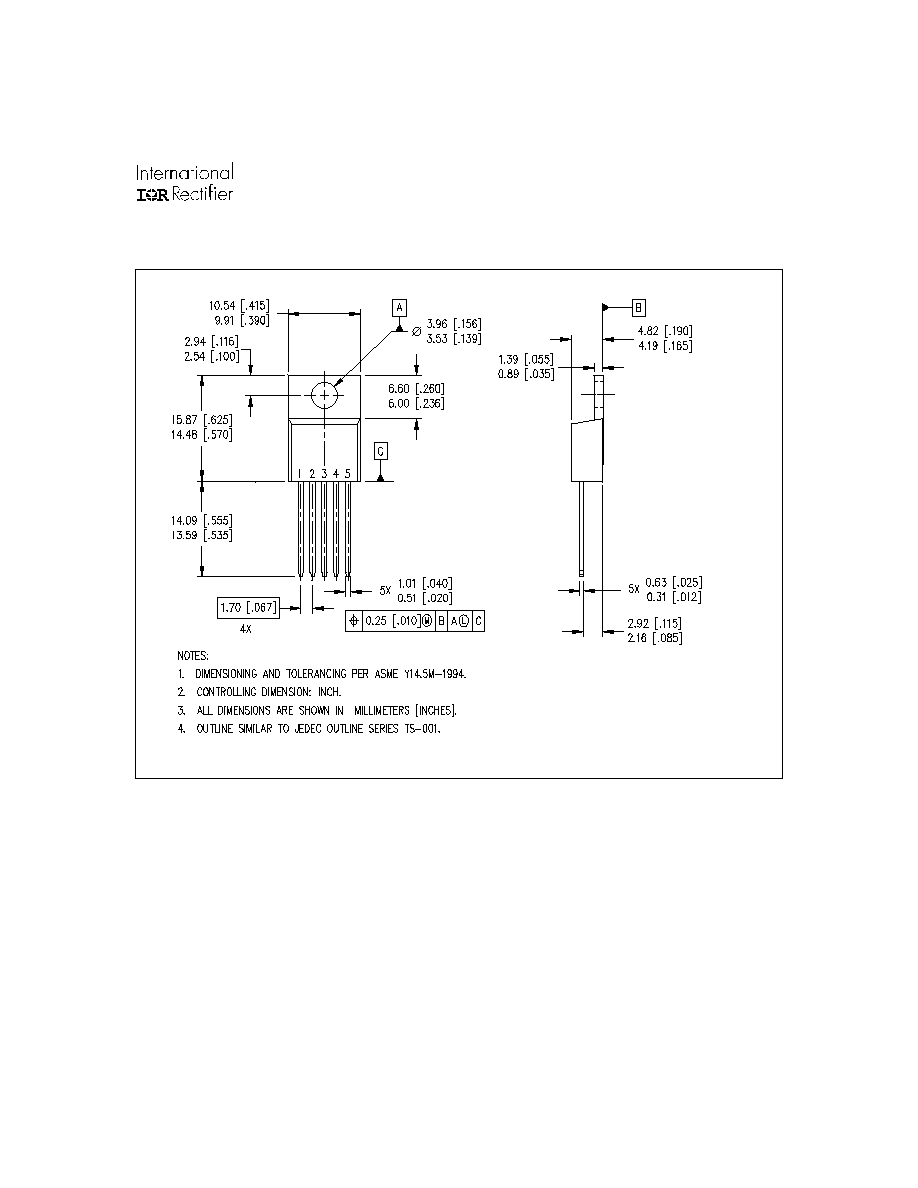
5-Lead TO-220
Case outline
01-6020 00
01-3042 01
(TS-001)