 | –≠–ª–µ–∫—Ç—Ä–æ–Ω–Ω—ã–π –∫–æ–º–ø–æ–Ω–µ–Ω—Ç: IRL3302 | –°–∫–∞—á–∞—Ç—å:  PDF PDF  ZIP ZIP |
9/17/97
IRL3302S
PRELIMINARY
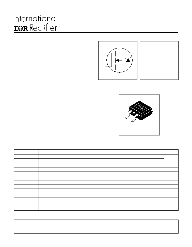
HEXFET
Æ
Power MOSFET
PD - 9.1692A
S
D
G
V
DSS
= 20V
R
DS(on)
= 0.020
W
I
D
= 39A
Description
Parameter
Typ.
Max.
Units
R
q
JC
Junction-to-Case
≠≠≠
2.2
R
q
JA
Junction-to-Ambient ( PCB Mounted,steady-state)**
≠≠≠
40
∞C/W
Thermal Resistance
Parameter
Max.
Units
I
D
@ T
C
= 25∞C
Continuous Drain Current, V
GS
@ 4.5V
39
I
D
@ T
C
= 100∞C
Continuous Drain Current, V
GS
@ 4.5V
25
A
I
DM
Pulsed Drain Current
160
P
D
@T
C
= 25∞C
Power Dissipation
57
W
Linear Derating Factor
0.45
W/∞C
V
GS
Gate-to-Source Voltage
± 10
V
E
AS
Single Pulse Avalanche Energy
130
mJ
I
AR
Avalanche Current
23
A
E
AR
Repetitive Avalanche Energy
5.7
mJ
dv/dt
Peak Diode Recovery dv/dt
5.0
V/ns
T
J
Operating Junction and
-55 to + 150
T
STG
Storage Temperature Range
Soldering Temperature, for 10 seconds
300 (1.6mm from case )
∞C
Absolute Maximum Ratings
These HEXFET Power MOSFETs were designed
specifically to meet the demands of CPU core DC-DC
converters. Advanced processing techniques
combined with an optimized gate oxide design results
in a die sized specifically to offer maximum efficiency
at minimum cost.
The D
2
Pak is a surface mount power package capable
of accommodating die sizes up to HEX-4. It provides the
highest power capability and the lowest possible on-
resistance in any existing surface mount package. The
D
2
Pak is suitable for high current applications because
of its low internal connection resistance and can
dissipate up to 2.0W in a typical surface mount
application.
2
D P a k
l
Advanced Process Technology
l
Surface Mount
l
Optimized for 4.5V-7.0V Gate Drive
l
Ideal for CPU Core DC-DC Converters
l
Fast Switching

IRL3302S
Repetitive rating; pulse width limited by
max. junction temperature.
I
SD
£
23A, di/dt
£
97A/µs, V
DD
£
V
(BR)DSS
,
T
J
£
150∞C
Notes:
Starting T
J
= 25∞C, L = 0.49mH
R
G
= 25
W
, I
AS
= 23A.
Pulse width
£
300µs; duty cycle
£
2%.
S
D
G
Parameter
Min. Typ. Max. Units
Conditions
I
S
Continuous Source Current
MOSFET symbol
(Body Diode)
≠≠≠
≠≠≠
showing the
I
SM
Pulsed Source Current
integral reverse
(Body Diode)
≠≠≠
≠≠≠
p-n junction diode.
V
SD
Diode Forward Voltage
≠≠≠
≠≠≠
1.3
V
T
J
= 25∞C, I
S
= 23A, V
GS
= 0V
t
rr
Reverse Recovery Time
≠≠≠
62
94
ns
T
J
= 25∞C, I
F
= 23A
Q
rr
Reverse Recovery
Charge ≠≠≠
110
160
nC
di/dt = 100A/µs
t
on
Forward Turn-On Time
Intrinsic turn-on time is negligible (turn-on is dominated by L
S
+L
D
)
Source-Drain Ratings and Characteristics
39
160
A
Parameter
Min. Typ. Max. Units
Conditions
V
(BR)DSS
Drain-to-Source Breakdown Voltage
20
≠≠≠
≠≠≠
V
V
GS
= 0V, I
D
= 250µA
D
V
(BR)DSS
/
D
T
J
Breakdown Voltage Temp. Coefficient
≠≠≠
0.022 ≠≠≠
V/∞C
Reference to 25∞C, I
D
= 1mA
≠≠≠
≠≠≠ 0.023
V
GS
= 4.5V, I
D
= 23A
≠≠≠
≠≠≠ 0.020
W
V
GS
= 7.0V, I
D
= 23A
V
GS(th)
Gate Threshold Voltage
0.70
≠≠≠
≠≠≠
V
V
DS
= V
GS
, I
D
= 250µA
g
fs
Forward Transconductance
21
≠≠≠
≠≠≠
S
V
DS
= 10V, I
D
= 23A
≠≠≠
≠≠≠
25
µA
V
DS
= 20V, V
GS
= 0V
≠≠≠
≠≠≠
250
V
DS
= 10V, V
GS
= 0V, T
J
= 150∞C
Gate-to-Source Forward Leakage
≠≠≠
≠≠≠
100
nA
V
GS
= 10V
Gate-to-Source Reverse Leakage
≠≠≠
≠≠≠
-100
V
GS
= -10V
Q
g
Total Gate Charge
≠≠≠
≠≠≠
31
I
D
= 23A
Q
gs
Gate-to-Source Charge
≠≠≠
≠≠≠
5.7
nC
V
DS
= 16V
Q
gd
Gate-to-Drain ("Miller") Charge
≠≠≠
≠≠≠
13
V
GS
= 4.5V, See Fig. 6
t
d(on)
Turn-On Delay Time
≠≠≠
7.2
≠≠≠
V
DD
= 10V
t
r
Rise Time
≠≠≠
110
≠≠≠
ns
I
D
= 23A
t
d(off)
Turn-Off Delay Time
≠≠≠
41
≠≠≠
R
G
= 9.5
W,
V
GS
= 4.5V
t
f
Fall Time
≠≠≠
89
≠≠≠
R
D
= 2.4
W,
Between lead,
and center of die contact
C
iss
Input Capacitance
≠≠≠
1300 ≠≠≠
V
GS
= 0V
C
oss
Output Capacitance
≠≠≠
520
≠≠≠
pF
V
DS
= 15V
C
rss
Reverse Transfer Capacitance
≠≠≠
190
≠≠≠
= 1.0MHz, See Fig. 5
Electrical Characteristics @ T
J
= 25∞C (unless otherwise specified)
R
DS(on)
Static Drain-to-Source On-Resistance
I
GSS
nH
L
S
Internal Source Inductance
≠≠≠
7.5
≠≠≠
I
DSS
Drain-to-Source Leakage Current
Uses IRL3302 data and test conditions
** When mounted on FR-4 board using minimum recommended footprint.
For recommended footprint and soldering techniques refer to application note #AN-994.

IRL3302S
Fig 4. Normalized On-Resistance
Vs. Temperature
Fig 2. Typical Output Characteristics
Fig 1. Typical Output Characteristics
Fig 3. Typical Transfer Characteristics
-60 -40 -20
0
20
40
60
80 100 120 140 160
0.0
0.5
1.0
1.5
2.0
T , Junction Temperature( C)
R , Drain-to-Source On Resistance
(Normalized)
J
DS(on)
∞
V
=
I =
GS
D
4.5V
39A
10
100
1000
0.1
1
10
100
20µs PULSE WIDTH
T = 25 C
J
∞
TOP
BOTTOM
VGS
15V
12V
10V
8.0V
6.0V
4.0V
3.0V
2.5V
V , Drain-to-Source Voltage (V)
I , Drain-to-Source Current (A)
DS
D
2.5V
10
100
1000
0.1
1
10
100
20µs PULSE WIDTH
T = 150 C
J
∞
TOP
BOTTOM
VGS
15V
12V
10V
8.0V
6.0V
4.0V
3.0V
2.5V
V , Drain-to-Source Voltage (V)
I , Drain-to-Source Current (A)
DS
D
2.5V
1
10
100
1000
2
3
4
5
6
7
8
V = 15V
20µs PULSE WIDTH
DS
V , Gate-to-Source Voltage (V)
I , Drain-to-Source Current (A)
GS
D
T = 25 C
J
∞
T = 150 C
J
∞
VGS
TOP 10V
8.0V
6.0V
4.0V
3.0V
BOTTOM 2.5V
VGS
TOP 10V
8.0V
6.0V
4.0V
3.0V
BOTTOM 2.5V

IRL3302S
Fig 8. Maximum Safe Operating Area
Fig 6. Typical Gate Charge Vs.
Gate-to-Source Voltage
Fig 5. Typical Capacitance Vs.
Drain-to-Source Voltage
Fig 7. Typical Source-Drain Diode
Forward Voltage
1
10
100
0
400
800
1200
1600
2000
2400
V , Drain-to-Source Voltage (V)
C, Capacitance (pF)
DS
V
C
C
C
=
=
=
=
0V,
C
C
C
f = 1MHz
+ C
+ C
C SHORTED
GS
iss
gs
gd ,
ds
rss
gd
oss
ds
gd
C
iss
C
oss
C
rss
0
10
20
30
40
50
0
3
6
9
12
15
Q , Total Gate Charge (nC)
V , Gate-to-Source Voltage (V)
G
GS
I =
D
23A
V
= 16V
DS
1
10
100
1000
0.5
1.0
1.5
2.0
V ,Source-to-Drain Voltage (V)
I , Reverse Drain Current (A)
SD
SD
V = 0 V
GS
T = 25 C
J
∞
T = 150 C
J
∞
1
10
100
1000
1
10
100
OPERATION IN THIS AREA LIMITED
BY R
DS(on)
Single Pulse
T
T
= 150 C
= 25 C
∞
∞
J
C
V , Drain-to-Source Voltage (V)
I , Drain Current (A)
I , Drain Current (A)
DS
D
10us
100us
1ms
10ms

IRL3302S
Fig 11. Maximum Effective Transient Thermal Impedance, Junction-to-Case
Fig 9. Maximum Drain Current Vs.
Case Temperature
Fig 10. Maximum Avalanche Energy
Vs. Drain Current
25
50
75
100
125
150
0
10
20
30
40
T , Case Temperature ( C)
I , Drain Current (A)
∞
C
D
25
50
75
100
125
150
0
50
100
150
200
250
300
Starting T , Junction Temperature( C)
E , Single Pulse Avalanche Energy (mJ)
J
AS
∞
ID
TOP
BOTTOM
10A
15A
23A
0.01
0.1
1
10
0.00001
0.0001
0.001
0.01
0.1
1
Notes:
1. Duty factor D = t / t
2. Peak T = P
x Z
+ T
1
2
J
DM
thJC
C
P
t
t
DM
1
2
t , Rectangular Pulse Duration (sec)
Thermal Response
(Z )
1
thJC
0.01
0.02
0.05
0.10
0.20
D = 0.50
SINGLE PULSE
(THERMAL RESPONSE)