 | ÐлекÑÑоннÑй компоненÑ: IRL3502 | СкаÑаÑÑ:  PDF PDF  ZIP ZIP |
Äîêóìåíòàöèÿ è îïèñàíèÿ www.docs.chipfind.ru
Parameter
Max.
Units
I
D
@ T
C
= 25°C
Continuous Drain Current, V
GS
@ 5.0V
110
I
D
@ T
C
= 100°C
Continuous Drain Current, V
GS
@ 5.0V
67
A
I
DM
Pulsed Drain Current
420
P
D
@T
C
= 25°C
Power Dissipation
140
W
Linear Derating Factor
1.1
W/°C
V
GS
Gate-to-Source Voltage
± 10
V
V
GSM
Gate-to-Source Voltage
14
V
(Start Up Transient, tp = 100µs)
E
AS
Single Pulse Avalanche Energy
390
mJ
I
AR
Avalanche Current
64
A
E
AR
Repetitive Avalanche Energy
14
mJ
dv/dt
Peak Diode Recovery dv/dt
5.0
V/ns
T
J
Operating Junction and
-55 to + 150
T
STG
Storage Temperature Range
Soldering Temperature, for 10 seconds
300 (1.6mm from case )
°C
Mounting torque, 6-32 or M3 srew
10 lbf·in (1.1N·m)
11/17/97
IRL3502
PRELIMINARY
HEXFET
®
Power MOSFET
PD 9.1698A
These HEXFET Power MOSFETs were designed
specifically to meet the demands of CPU core DC-DC
converters. Advanced processing techniques
combined with an optimized gate oxide design results
in a die sized specifically to offer maximum efficiency
at minimum cost.
The TO-220 package is universally preferred for all
commercial-industrial applications at power dissipation
levels to approximately 50 watts. The low thermal
resistance and low package cost of the TO-220
contribute to its wide acceptance throughout the
industry.
S
D
G
Absolute Maximum Ratings
Parameter
Typ.
Max.
Units
R
JC
Junction-to-Case
0.89
R
CS
Case-to-Sink, Flat, Greased Surface
0.50
°C/W
R
JA
Junction-to-Ambient
62
Thermal Resistance
V
DSS
= 20V
R
DS(on)
= 0.007
I
D
= 110A
TO-220AB
Description
l
Advanced Process Technology
l
Optimized for 4.5V-7.0V Gate Drive
l
Ideal for CPU Core DC-DC Converters
l
Fast Switching
IRL3502
Parameter
Min. Typ. Max. Units
Conditions
V
(BR)DSS
Drain-to-Source Breakdown Voltage
20
V
V
GS
= 0V, I
D
= 250µA
V
(BR)DSS
/
T
J
Breakdown Voltage Temp. Coefficient
0.019
V/°C
Reference to 25°C, I
D
= 1mA
0.008
V
GS
= 4.5V, I
D
= 64A
0.007
V
GS
= 7.0V, I
D
= 64A
V
GS(th)
Gate Threshold Voltage
0.70
V
V
DS
= V
GS
, I
D
= 250µA
g
fs
Forward Transconductance
77
S
V
DS
= 10V, I
D
= 64A
25
µA
V
DS
= 20V, V
GS
= 0V
250
V
DS
= 10V, V
GS
= 0V, T
J
= 150°C
Gate-to-Source Forward Leakage
100
nA
V
GS
= -10V
Gate-to-Source Reverse Leakage
-100
V
GS
= 10V
Q
g
Total Gate Charge
110
I
D
= 64A
Q
gs
Gate-to-Source Charge
27
nC
V
DS
= 16V
Q
gd
Gate-to-Drain ("Miller") Charge
39
V
GS
= 4.5V, See Fig. 6
t
d(on)
Turn-On Delay Time
10
V
DD
= 10V
t
r
Rise Time
140
ns
I
D
= 64A
t
d(off)
Turn-Off Delay Time
96
R
G
= 3.8
,
V
GS
= 4.5V
t
f
Fall Time
130
R
D
= 0.15
,
Between lead,
6mm (0.25in.)
from package
and center of die contact
C
iss
Input Capacitance
4700
V
GS
= 0V
C
oss
Output Capacitance
1900
pF
V
DS
= 15V
C
rss
Reverse Transfer Capacitance
640
= 1.0MHz, See Fig. 5
S
D
G
S
D
G
Parameter
Min. Typ. Max. Units
Conditions
I
S
Continuous Source Current
MOSFET symbol
(Body Diode)
showing the
I
SM
Pulsed Source Current
integral reverse
(Body Diode)
p-n junction diode.
V
SD
Diode Forward Voltage
1.3
V
T
J
= 25°C, I
S
= 64A, V
GS
= 0V
t
rr
Reverse Recovery Time
87
130
ns
T
J
= 25°C, I
F
= 64A
Q
rr
Reverse RecoveryCharge
200
310
nC
di/dt = 100A/µs
t
on
Forward Turn-On Time
Intrinsic turn-on time is negligible (turn-on is dominated by L
S
+L
D
)
Source-Drain Ratings and Characteristics
110
420
A
Electrical Characteristics @ T
J
= 25°C (unless otherwise specified)
R
DS(on)
Static Drain-to-Source On-Resistance
I
GSS
nH
L
S
Internal Source Inductance
7.5
L
D
Internal Drain Inductance
4.5
I
DSS
Drain-to-Source Leakage Current
Repetitive rating; pulse width limited by
max. junction temperature.
I
SD
64A, di/dt
86A/µs, V
DD
V
(BR)DSS
,
T
J
150°C
Notes:
Starting T
J
= 25°C, L = 190µH
R
G
= 25
, I
AS
= 64A.
Pulse width
300µs; duty cycle
2%.
Calculated continuous current based on maximum allowable
junction temperature; for recommended current-handling of the
package refer to Design Tip # 93-4
IRL3502
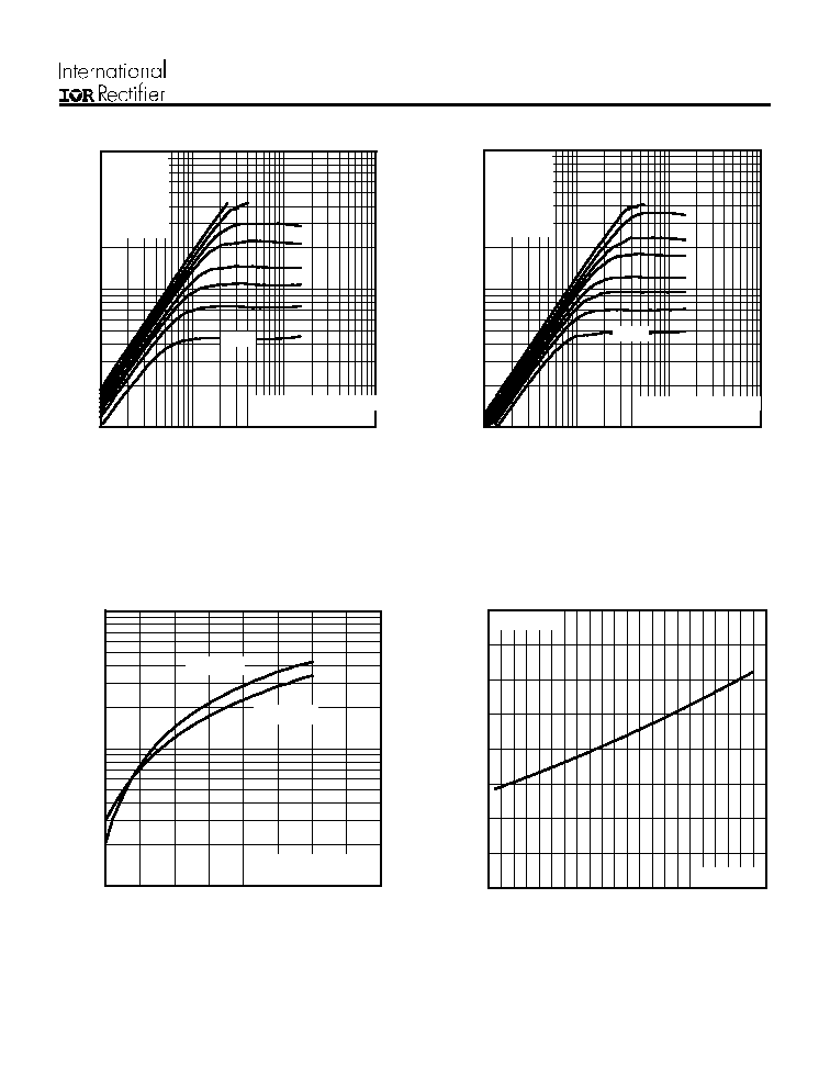
Fig 4. Normalized On-Resistance
Vs. Temperature
Fig 2. Typical Output Characteristics
Fig 1. Typical Output Characteristics
Fig 3. Typical Transfer Characteristics
10
100
1000
2
3
4
5
6
V = 15V
20µs PULSE WIDTH
DS
V , Gate-to-Source Voltage (V)
I , Drain-to-Source Current (A)
GS
D
T = 25 C
J
°
T = 150 C
J
°
-60 -40 -20
0
20
40
60
80 100 120 140 160
0.0
0.5
1.0
1.5
2.0
T , Junction Temperature( C)
R , Drain-to-Source On Resistance
(Normalized)
J
DS(on)
°
V
=
I =
GS
D
4.5V
110A
10
100
1000
0.1
1
10
100
20µs PULSE WIDTH
T = 25 C
J
°
TOP
BOTTOM
VGS
7.00V
5.00V
4.50V
3.50V
3.00V
2.70V
2.50V
2.25V
V , Drain-to-Source Voltage (V)
I , Drain-to-Source Current (A)
DS
D
2.25V
10
100
1000
0.1
1
10
100
20µs PULSE WIDTH
T = 150 C
J
°
TOP
BOTTOM
VGS
7.00V
5.00V
4.50V
3.50V
3.00V
2.70V
2.50V
2.25V
V , Drain-to-Source Voltage (V)
I , Drain-to-Source Current (A)
DS
D
2.25V
IRL3502
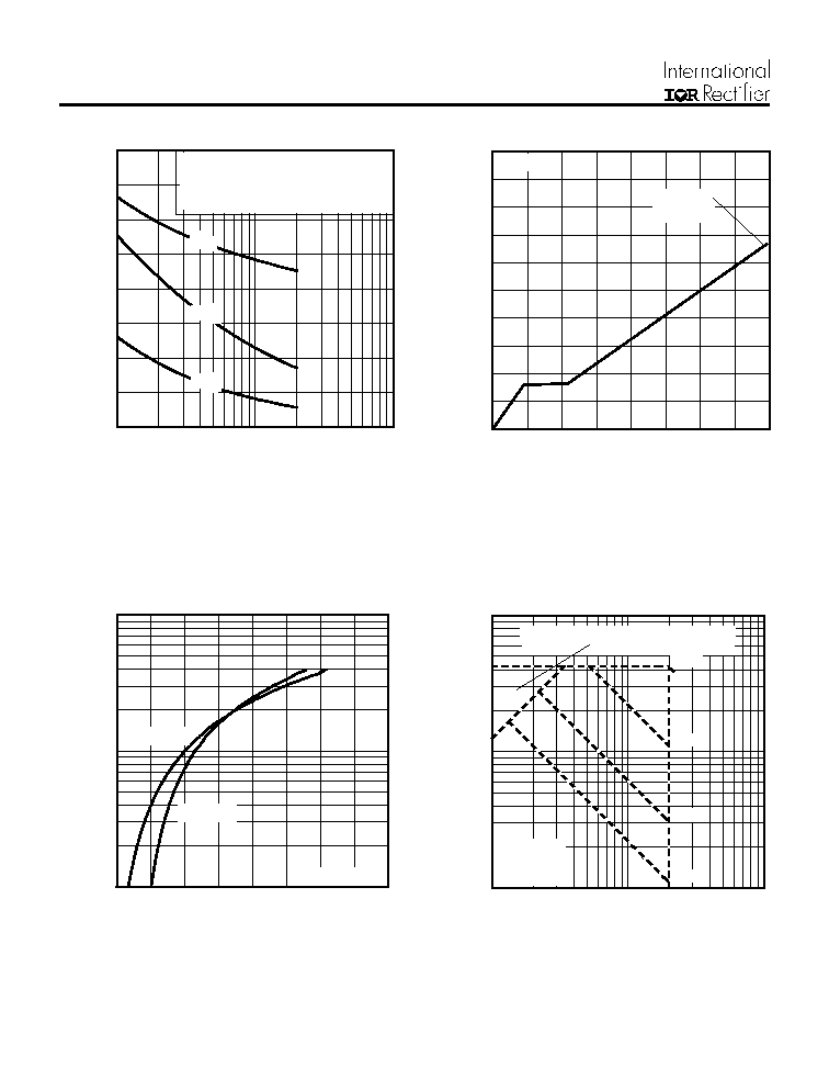
Fig 8. Maximum Safe Operating Area
Fig 6. Typical Gate Charge Vs.
Gate-to-Source Voltage
Fig 5. Typical Capacitance Vs.
Drain-to-Source Voltage
Fig 7. Typical Source-Drain Diode
Forward Voltage
1
10
100
0
2000
4000
6000
8000
V , Drain-to-Source Voltage (V)
C, Capacitance (pF)
DS
V
C
C
C
=
=
=
=
0V,
C
C
C
f = 1MHz
+ C
+ C
C SHORTED
GS
iss
gs
gd ,
ds
rss
gd
oss
ds
gd
C
iss
C
oss
C
rss
10
100
1000
0.5
1.0
1.5
2.0
2.5
V ,Source-to-Drain Voltage (V)
I , Reverse Drain Current (A)
SD
SD
V = 0 V
GS
T = 25 C
J
°
T = 150 C
J
°
10
100
1000
1
10
100
OPERATION IN THIS AREA LIMITED
BY R
DS(on)
Single Pulse
T
T
= 150 C
= 25 C
°
°
J
C
V , Drain-to-Source Voltage (V)
I , Drain Current (A)
I , Drain Current (A)
DS
D
10us
100us
1ms
10ms
0
40
80
120
160
0
3
6
9
12
15
Q , Total Gate Charge (nC)
V , Gate-to-Source Voltage (V)
G
GS
I =
D
64A
V
= 16V
DS
IRL3502
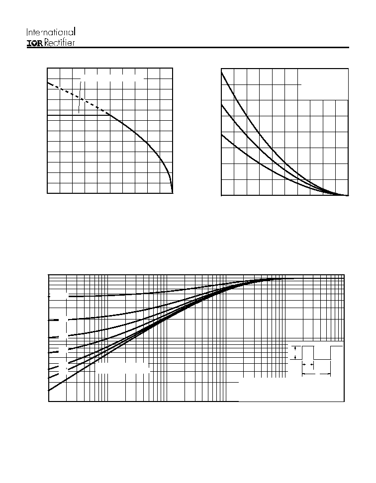
Fig 11. Maximum Effective Transient Thermal Impedance, Junction-to-Case
Fig 9. Maximum Drain Current Vs.
Case Temperature
Fig 10. Maximum Avalanche Energy
Vs. Drain Current
25
50
75
100
125
150
0
20
40
60
80
100
120
T , Case Temperature ( C)
I , Drain Current (A)
°
C
D
LIMITED BY PACKAGE
25
50
75
100
125
150
0
200
400
600
800
Starting T , Junction Temperature( C)
E , Single Pulse Avalanche Energy (mJ)
J
AS
°
ID
TOP
BOTTOM
29A
40A
64A
0.01
0.1
1
0.00001
0.0001
0.001
0.01
0.1
1
Notes:
1. Duty factor D = t / t
2. Peak T = P
x Z
+ T
1
2
J
DM
thJC
C
P
t
t
DM
1
2
t , Rectangular Pulse Duration (sec)
Thermal Response
(Z )
1
thJC
0.01
0.02
0.05
0.10
0.20
D = 0.50
SINGLE PULSE
(THERMAL RESPONSE)