 | ÐлекÑÑоннÑй компоненÑ: IRL620S | СкаÑаÑÑ:  PDF PDF  ZIP ZIP |
Äîêóìåíòàöèÿ è îïèñàíèÿ www.docs.chipfind.ru
Parameter
Max.
Units
I
D
@ T
C
= 25°C
Continuous Drain Current, V
GS
@ 5.0 V
5.2
I
D
@ T
C
= 100°C
Continuous Drain Current, V
GS
@ 5.0 V
3.3
A
I
DM
Pulsed Drain Current
21
P
D
@T
C
= 25°C
Power Dissipation
50
P
D
@T
A
= 25°C
Power Dissipation (PCB Mount)**
3.1
Linear Derating Factor
0.40
Linear Derating Factor (PCB Mount)**
0.025
V
GS
Gate-to-Source Voltage
±10
V
E
AS
Single Pulse Avalanche Energy
125
mJ
I
AR
Avalanche Current
5.2
A
E
AR
Repetitive Avalanche Energy
5.0
mJ
dv/dt
Peak Diode Recovery dv/dt
5.0
V/ns
T
J,
T
STG
Junction and Storage Temperature Range
-55 to + 150
Soldering Temperature, for 10 seconds
300 (1.6mm from case)
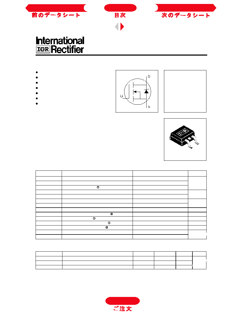
IRL620S
HEXFET
®
Power MOSFET
PD -9.1218
Revision 0
V
DSS
= 200V
R
DS(on)
= 0.80
I
D
= 5.2A
Absolute Maximum Ratings
Thermal Resistance
Parameter
Min.
Typ.
Max.
Units
R
JC
Junction-to-Case
--
--
2.5
R
JA
Junction-to-Ambient (PCB Mount)**
--
--
40
°C/W
R
JA
Junction-to-Ambient
--
--
62
Surface Mount
Available in Tape & Reel
Dynamic dv/dt Rating
Repetitive Avalanche Rated
Logic-Level Gate Drive
R
DS(on)
Specified at V
GS
=4V & 5V
Fast Switching
Third Generation HEXFETs from International Rectifier provide the designer
with the best combination of fast switching, ruggedized device design, low on-
resistance and cost-effectiveness.
The SMD-220 is a surface-mount power package capable of accommodating die
sizes up to HEX-4. It provides the highest power capability and the lowest possible
on-resistance in any existing surface-mount package. The SMD-220 is suitable for
high current applications because of its low internal connection resistance and can
dissipate up to 2.0W in a typical surface-mount application.
Description
A
SMD-220
W
W/°C
°C
** When mounted on 1" square PCB (FR-4 or G-10 Material). For recommended footprint and soldering techniques, refer
to Application Note AN-994.
Next Data Sheet
Index
Previous Datasheet
To Order
Parameter
Min. Typ. Max. Units Conditions
V
(BR)DSS
Drain-to-Source Breakdown Voltage
200
--
--
V
V
GS
= 0V, ID = 250µA
V
(BR)DSS
/
T
J
Breakdown Voltage Temp. Coefficient
--
0.27
--
V/°C Reference to 25°C, I
D
= 1mA
R
DS(on)
Static Drain-to-Source On-Resistance
--
--
0.80
V
GS
= 10.0V, I
D
= 3.1A
--
--
1.0
V
GS
= 4.0V, I
D
= 2.6A
V
GS(th)
Gate Threshold Voltage
1.0
--
2.0
V
V
DS
= V
GS
, I
D
= 250µA
g
fs
Forward Transconductance
1.2
--
--
S
V
DS
= 50V, I
D
= 3.1A
I
DSS
Drain-to-Source Leakage Current
--
--
25
V
DS
= 200V, V
GS
= 0V
--
--
250
V
DS
= 320V, V
GS
= 0V, T
J
= 125°C
I
GSS
Gate-to-Source Forward Leakage
--
--
100
V
GS
= 10V
Gate-to-Source Reverse Leakage
--
--
-100
V
GS
= -10V
Q
g
Total Gate Charge
--
--
16
I
D
= 5.2A
Q
gs
Gate-to-Source Charge
--
--
2.9
nC
V
DS
= 160V
Q
gd
Gate-to-Drain ("Miller") Charge
--
--
9.6
V
GS
= 5.0V, See Fig. 6 and 13
t
d(on)
Turn-On Delay Time
--
4.2
--
V
DD
= 100V
t
r
Rise Time
--
31
--
I
D
= 5.2A
t
d(off)
Turn-Off Delay Time
--
18
--
R
G
= 9.0
t
f
Fall Time
--
17
--
R
D
= 20
,
See Fig. 10
L
D
Internal Drain Inductance
--
4.5
--
Between lead,
6mm (0.25in.)
L
S
Internal Source Inductance
--
7.5
--
from package
and center of
die contact
C
iss
Input Capacitance
--
360
--
V
GS
= 0V
C
oss
Output Capacitance
--
91
--
pF
V
DS
= 25V
C
rss
Reverse Transfer Capacitance
--
27
--
= 1.0MHz, See Fig. 5
IRL620S
Notes:
Parameter
Min. Typ. Max. Units Conditions
I
S
Continuous Source Current
MOSFET symbol
(Body Diode)
showing the
I
SM
Pulsed Source Current
integral reverse
(Body Diode)
p-n junction diode.
V
SD
Diode Forward Voltage
--
--
1.8
V
T
J
= 25°C, I
S
= 5.2A, V
GS
= 0V
t
rr
Reverse Recovery Time
--
180
270
ns
T
J
= 25°C, I
F
= 5.2A
Q
rr
Reverse RecoveryCharge
--
1.1
1.7
µC
di/dt = 100A/µs
t
on
Forward Turn-On Time
Repetitive rating; pulse width limited by
max. junction temperature. ( See fig. 11 )
V
DD
= 50V, starting T
J
= 25°C, L = 6.9mH
R
G
= 25
, I
AS
= 5.2A. (See Figure 12)
I
SD
5.2A, di/dt
95A/µs, V
DD
V
(BR)DSS
,
T
J
150°C
Pulse width
300µs; duty cycle
2%.
Source-Drain Ratings and Characteristics
Electrical Characteristics @ T
J
= 25°C (unless otherwise specified)
Intrinsic turn-on time is negligible (turn-on is dominated by L
S
+L
D
)
--
--
21
--
--
5.2
A
ns
nA
µA
nH
Next Data Sheet
Index
Previous Datasheet
To Order
Fig 3. Typical Transfer Characteristics
Fig 4. Normalized On-Resistance
Vs. Temperature
IRL620S
Fig 1. Typical Output Characteristics,
T
C
= 25
o
C
Fig 2. Typical Output Characteristics,
T
C
= 150
o
C
R
D
S
(
o
n
)
,
D
r
a
i
n
-
t
o
-
S
o
u
r
c
e
O
n
R
e
s
i
s
t
a
n
c
e
(
N
o
r
m
a
l
i
z
e
d
)
I
D
,
D
r
a
i
n
C
u
r
r
e
n
t
(
A
m
p
s
)
I
D
,
D
r
a
i
n
C
u
r
r
e
n
t
(
A
m
p
s
)
I
D
,
D
r
a
i
n
C
u
r
r
e
n
t
(
A
m
p
s
)
To Order
Next Data Sheet
Index
Previous Datasheet
IRL620s
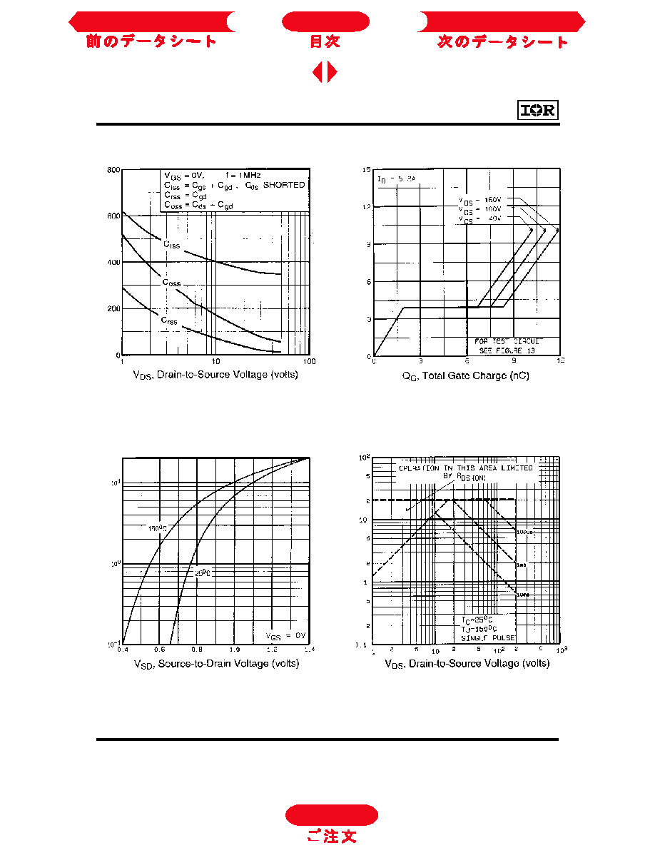
Fig 7. Typical Source-Drain Diode
Forward Voltage
Fig 8. Maximum Safe Operating Area
Fig 5. Typical Capacitance Vs.
Drain-to-Source Voltage
Fig 6. Typical Gate Charge Vs.
Gate-to-Source Voltage
C
a
p
a
c
i
t
a
n
c
e
(
p
F
)
V
G
S
,
G
a
t
e
-
t
o
-
S
o
u
r
c
e
V
o
l
t
a
g
e
(
v
o
l
t
s
)
I
S
D
,
R
e
v
e
r
s
e
D
r
a
i
n
C
u
r
r
e
n
t
(
A
m
p
s
)
I
D
,
D
r
a
i
n
C
u
r
r
e
n
t
(
A
m
p
s
)
To Order
Next Data Sheet
Index
Previous Datasheet
IRL620S
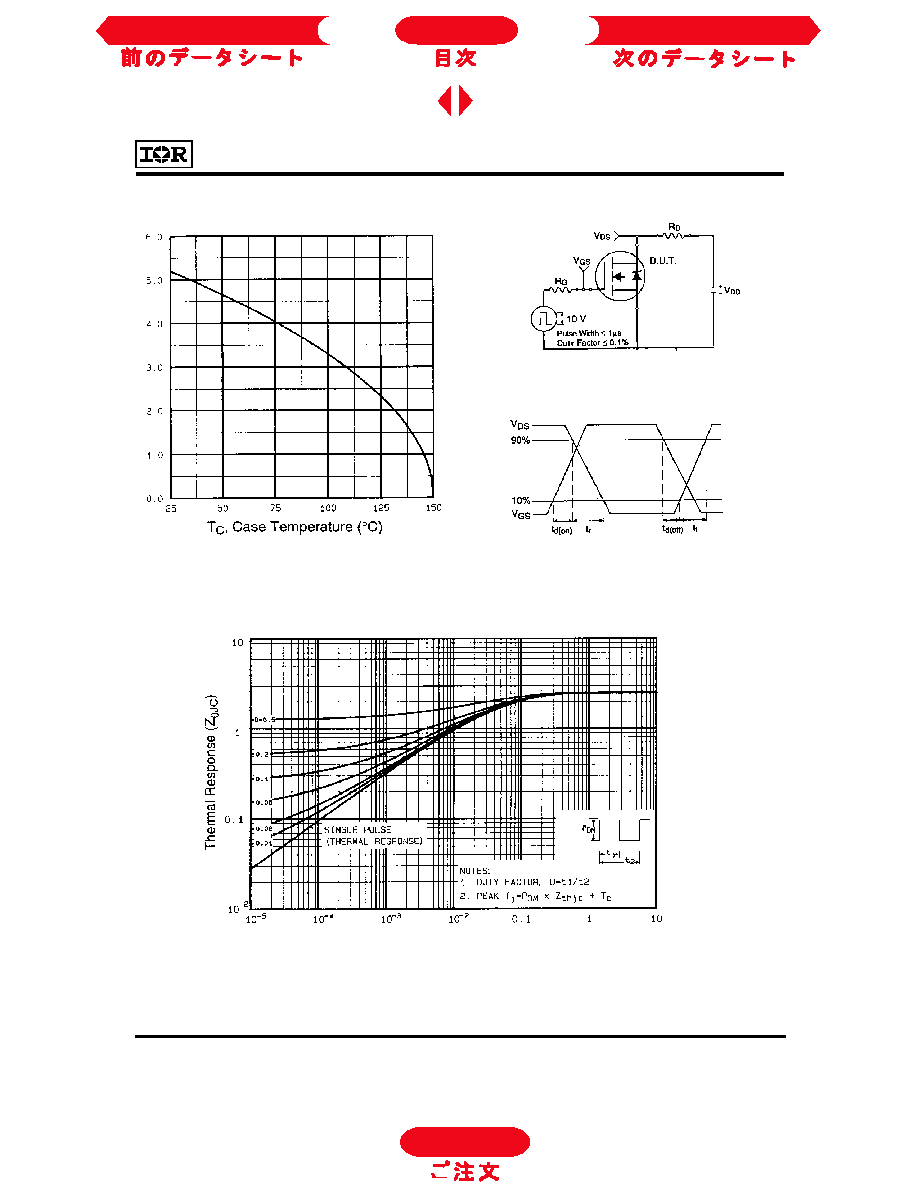
Fig 10a. Switching Time Test Circuit
Fig 9. Maximum Drain Current Vs.
Case Temperature
Fig 10b. Switching Time Waveforms
Fig 11. Maximum Effective Transient Thermal Impedance, Junction-to-Case
I
D
,
D
r
a
i
n
C
u
r
r
e
n
t
(
A
m
p
s
)
To Order
Next Data Sheet
Index
Previous Datasheet