 | –≠–ª–µ–∫—Ç—Ä–æ–Ω–Ω—ã–π –∫–æ–º–ø–æ–Ω–µ–Ω—Ç: IRL630 | –°–∫–∞—á–∞—Ç—å:  PDF PDF  ZIP ZIP |

IRL630
HEXFET
Æ
Power MOSFET
PD -9.1255
Revision 0
V
DSS
= 200V
R
DS(on)
= 0.40
I
D
= 9.0A
Absolute Maximum Ratings
Thermal Resistance
Parameter
Max.
Units
I
D
@ T
C
= 25∞C
Continuous Drain Current, V
GS
@ 5.0V
9.0
I
D
@ T
C
= 100∞C
Continuous Drain Current, V
GS
@ 5.0V
5.7
A
I
DM
Pulsed Drain Current
36
P
D
@T
C
= 25∞C
Power Dissipation
74
W
Linear Derating Factor
0.59
W/∞C
V
GS
Gate-to-Source Voltage
±10
V
E
AS
Single Pulse Avalanche Energy
250
mJ
I
AR
Avalanche Current
9.0
A
E
AR
Repetitive Avalanche Energy
7.4
mJ
dv/dt
Peak Diode Recovery dv/dt
5.0
V/ns
T
J
Operating Junction and
-55 to + 150
T
STG
Storage Temperature Range
∞C
Soldering Temperature, for 10 seconds
300 (1.6mm from case)
Mounting torque, 6-32 or M3 screw.
10 lbf∑in (1.1N∑m)
Parameter
Min.
Typ.
Max.
Units
R
JC
Junction-to-Case
≠≠≠≠
≠≠≠≠
1.7
R
CS
Case-to-Sink, Flat, Greased Surface
≠≠≠≠
0.50
≠≠≠≠
∞C/W
R
JA
Junction-to-Ambient
≠≠≠≠
≠≠≠≠
62
Dynamic dv/dt Rating
Repetitive Avalanche Rated
Logic-Level Gate Drive
R
DS(ON)
Specified at V
GS
= 4V & 5V
150∞C Operating Temperature
Fast Switching
Ease of paralleling
Third Generation HEXFETs from International Rectifier provide the designer
with the best combination of fast switching, ruggedized device design, low on-
resistance and cost-effectiveness.
The TO-220 package is universally preferred for all commercial-industrial
applications at power dissipation levels to approximately 50 watts. The low
thermal resistance and low package cost of the TO-220 contribute to its wide
acceptance throughout the industry.
Description
Next Data Sheet
Index
Previous Datasheet
To Order

IRL630
Notes:
Parameter
Min. Typ. Max. Units
Conditions
I
S
Continuous Source Current
MOSFET symbol
(Body Diode)
showing the
I
SM
Pulsed Source Current
integral reverse
(Body Diode)
p-n junction diode.
V
SD
Diode Forward Voltage
≠≠≠
≠≠≠
2.0
V
T
J
= 25∞C, I
S
= 9.0A, V
GS
= 0V
t
rr
Reverse Recovery Time
≠≠≠
230
350
ns
T
J
= 25∞C, I
F
= 9.0A
Q
rr
Reverse Recovery Charge
≠≠≠
1.7
2.6
µC
di/dt = 100A/µs
t
on
Forward Turn-On Time
Repetitive rating; pulse width limited by
max. junction temperature. ( See fig. 11 )
V
DD
= 25V, starting T
J
= 25∞C, L = 4.6mH
R
G
= 25
, I
AS
= 9.0A. (See Figure 12)
I
SD
9.0A, di/dt
120A/µs, V
DD
V
(BR)DSS
,
T
J
150∞C
Pulse width
300µs; duty cycle
2%.
Source-Drain Ratings and Characteristics
Electrical Characteristics @ T
J
= 25∞C (unless otherwise specified)
Parameter
Min. Typ. Max. Units
Conditions
V
(BR)DSS
Drain-to-Source Breakdown Voltage
200
≠≠≠
≠≠≠
V
V
GS
= 0V, ID = 250µA
V
(BR)DSS
/
T
J
Breakdown Voltage Temp. Coefficient
≠≠≠ 0.27
≠≠≠
V/∞C
Reference to 25∞C, I
D
= 1mA
≠≠≠
≠≠≠ 0.40
V
GS
= 5.0V, I
D
= 5.4A
≠≠≠
≠≠≠ 0.50
V
GS
= 4.0V, I
D
= 4.5A
V
GS(th)
Gate Threshold Voltage
1.0
≠≠≠
2.0
V
V
DS
= V
GS
, I
D
= 250µA
g
fs
Forward Transconductance
4.8
≠≠≠
≠≠≠
S
V
DS
= 50V, I
D
= 5.4A
≠≠≠
≠≠≠
25
V
DS
= 200V, V
GS
= 0V
≠≠≠
≠≠≠
250
V
DS
= 160V, V
GS
= 0V, T
J
= 125∞C
Gate-to-Source Forward Leakage
≠≠≠
≠≠≠
100
V
GS
= 10V
Gate-to-Source Reverse Leakage
≠≠≠
≠≠≠ -100
V
GS
= -10V
Q
g
Total Gate Charge
≠≠≠
≠≠≠
40
I
D
= 9.0A
Q
gs
Gate-to-Source Charge
≠≠≠
≠≠≠
5.5
nC
V
DS
= 160V
Q
gd
Gate-to-Drain ("Miller") Charge
≠≠≠
≠≠≠
24
V
GS
= 10V, See Fig. 6 and 13
t
d(on)
Turn-On Delay Time
≠≠≠
8.0
≠≠≠
V
DD
= 100V
t
r
Rise Time
≠≠≠
57
≠≠≠
I
D
= 9.0A
t
d(off)
Turn-Off Delay Time
≠≠≠
38
≠≠≠
R
G
= 6.0
t
f
Fall Time
≠≠≠
33
≠≠≠
R
D
= 11
,
See Fig. 10
Between lead,
6mm (0.25in.)
from package
and center of die contact
C
iss
Input Capacitance
≠≠≠ 1100 ≠≠≠
V
GS
= 0V
C
oss
Output Capacitance
≠≠≠
220
≠≠≠
pF
V
DS
= 25V
C
rss
Reverse Transfer Capacitance
≠≠≠
70
≠≠≠
= 1.0MHz, See Fig. 5
Intrinsic turn-on time is negligible (turn-on is dominated by L
S
+L
D
)
≠≠≠
≠≠≠
36
≠≠≠
≠≠≠
9.0
A
ns
I
DSS
Drain-to-Source Leakage Current
I
GSS
L
D
Internal Drain Inductance
≠≠≠
4.5
≠≠≠
L
S
Internal Source Inductance
≠≠≠
7.5
≠≠≠
nH
nA
µA
R
DS(ON)
Static Drain-to-Source On-Resistance
Next Data Sheet
Index
Previous Datasheet
To Order

Fig 3. Typical Transfer Characteristics
Fig 4. Normalized On-Resistance
Vs. Temperature
IRL630
Fig 1. Typical Output Characteristics,
T
C
= 25
o
C
Fig 2. Typical Output Characteristics,
T
C
= 150
o
C
0.1
1
1 0
1 0 0
0.1
1
1 0
10 0
I
,
D
r
a
i
n
-
t
o
-
S
o
u
r
c
e
C
u
r
r
e
n
t
(
A
)
D
V , Drain-to-Source Voltage (V)
DS
VGS
TOP 7.50V
5.00V
4.00V
3.50V
3.00V
2.75V
2.50V
BOTTOM 2.25V
2.25V
20µs PULSE WIDTH
T = 25∞C
c
A
0.01
0.1
1
10
100
2.0
2.5
3.0
3.5
4.0
4.5
5.0
T = 25∞C
T = 150∞C
J
J
GS
V , Gate-to-Source Voltage (V)
D
I
,
D
r
a
i
n
-
t
o
-
S
o
u
r
c
e
C
u
r
r
e
n
t
(
A
)
V = 50V
20µs PULSE WIDTH
DS
A
0.0
0.5
1.0
1.5
2.0
2.5
-60 -40 -20
0
20
40
60
80 100 120 140 160
J
T , Junction Temperature (∞C)
R
,
D
r
a
i
n
-
t
o
-
S
o
u
r
c
e
O
n
R
e
s
i
s
t
a
n
c
e
D
S
(
o
n
)
(
N
o
r
m
a
l
i
z
e
d
)
V = 5.0V
GS
I = 9.0A
D
A
I
,
D
r
a
i
n
-
t
o
-
S
o
u
r
c
e
C
u
r
r
e
n
t
(
A
)
D
To Order
Next Data Sheet
Index
Previous Datasheet

IRL630
Fig 7. Typical Source-Drain Diode
Forward Voltage
Fig 8. Maximum Safe Operating Area
Fig 5. Typical Capacitance Vs.
Drain-to-Source Voltage
Fig 6. Typical Gate Charge Vs.
Gate-to-Source Voltage
0
500
1000
1500
2000
1
10
100
C
,
C
a
p
a
c
i
t
a
n
c
e
(
p
F
)
DS
V , Drain-to-Source Voltage (V)
A
V = 0V, f = 1MHz
C = C + C , C SHORTED
C = C
C = C + C
GS
iss gs gd ds
rss gd
oss ds gd
C
iss
C
oss
C
rss
0
2
4
6
8
10
0
10
20
30
40
Q , Total Gate Charge (nC)
G
FOR TEST CIRCUIT
SEE FIGURE 13
V
,
G
a
t
e
-
t
o
-
S
o
u
r
c
e
V
o
l
t
a
g
e
(
V
)
G
S
I = 9.0A
V = 160V
V = 100V
V = 40V
D
DS
DS
DS
A
0.1
1
10
100
0
0.4
0.8
1.2
1.6
T = 25∞C
T = 150∞C
J
J
V = 0V
GS
V , Source-to-Drain Voltage (V)
I
,
R
e
v
e
r
s
e
D
r
a
i
n
C
u
r
r
e
n
t
(
A
)
SD
S
D
A
0 .1
1
1 0
1 0 0
1
1 0
1 0 0
1 0 0 0
V , Drain-to-Source Voltage (V)
DS
I
,
D
r
a
i
n
C
u
r
r
e
n
t
(
A
)
OPERATION IN THIS AREA LIMITED
BY R
D
DS(on)
T = 25∞C
T = 150∞C
Single Pulse
C
J
10µs
100µs
1ms
10ms
100ms
To Order
Next Data Sheet
Index
Previous Datasheet

IRL630
Fig 10a. Switching Time Test Circuit
V
DS
5.0 V
Pulse Width
1
µs
Duty Factor
0.1 %
Fig 9. Maximum Drain Current Vs.
Case Temperature
Fig 10b. Switching Time Waveforms
R
D
V
GS
V
DD
R
G
D.U.T.
Fig 11. Maximum Effective Transient Thermal Impedance, Junction-to-Case
0
2
4
6
8
10
25
50
75
100
125
150
C
I
,
D
r
a
i
n
C
u
r
r
e
n
t
(
A
m
p
s
)
D
T , Case Temperature (∞C)
A
0.01
0.1
1
10
0.00001
0.0001
0.001
0.01
0.1
1
10
t , Rectangular Pulse Duration (sec)
1
t
h
J
C
D = 0.50
0.01
0.02
0.05
0.10
0.20
SINGLE PULSE
(THERMAL RESPONSE)
T
h
e
r
m
a
l
R
e
s
p
o
n
s
e
(
Z
)
A
A
P
t
2
1
t
DM
N o te s :
1 . D u ty fa c to r D = t / t
2 . P e a k T = P x Z + T
1
2
J
D M
th J C
C
To Order
Next Data Sheet
Index
Previous Datasheet
IRL630
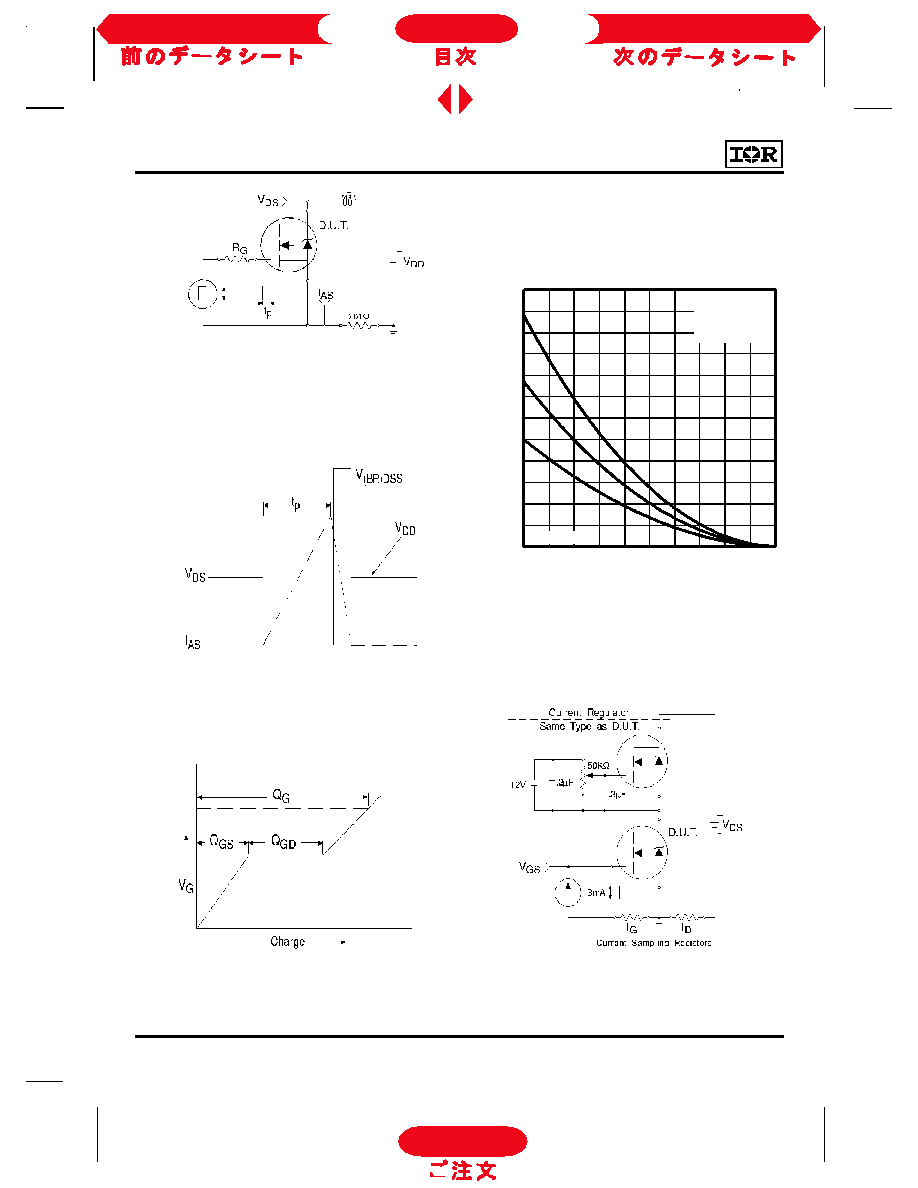
Fig 12a. Unclamped Inductive Test Circuit
5.0V
5.0V
Fig 13a. Basic Gate Charge Waveform
Fig 13b. Gate Charge Test Circuit
Fig 12b. Unclamped Inductive Waveforms
Fig 12c. Maximum Avalanche Energy
Vs. Drain Current
0
100
200
300
400
500
600
25
50
75
100
125
150
V = 50V
Starting T , Juntion Temperature (∞C)
J
E
,
S
i
n
g
l
e
P
u
l
s
e
A
v
a
l
a
n
c
h
e
E
n
e
r
g
y
(
m
J
)
A
S
DD
I
TOP 9.0A
5.7A
BOTTOM 4.0A
D
A
To Order
Next Data Sheet
Index
Previous Datasheet

IRL630
Fig 14. For N-Channel HEXFETS
*
VGS = 5V for Logic Level Devices
Peak Diode Recovery dv/dt Test Circuit
R
G
V
DD
∑
dv/dt controlled by R
G
∑
Driver same type as D.U.T.
∑
I
SD
controlled by Duty Factor "D"
∑
D.U.T. - Device Under Test
D.U.T
Circuit Layout Considerations
∑
Low Stray Inductance
∑
Ground Plane
∑
Low Leakage Inductance
Current Transformer
*
To Order
Next Data Sheet
Index
Previous Datasheet

IRL630
Package Outline
TO-220AB Outline
NOTES:
1 DIMENSIONS & TOLERANCING
PER ANSI Y14.5M, 1982.
2 CONTROLLING DIMENSION : INCH.
3 DIMENSIONS ARE SHOW N
MILLIMETERS (INCHES).
4 CONFORMS TO JEDEC OUTLINE
TO-220AB.
LEAD ASSIGNMENTS
1 - GATE
2 - DRAIN
3 - SOURCE
4 - DRAIN
0.55 (.022)
0.46 (.018)
3 X
1.32 (.052)
1.22 (.048)
- B -
4.69 (.185)
4.20 (.165)
3.78 (.149)
3.54 (.139)
- A -
6.47 (.255)
6.10 (.240)
1.15 (.045)
MIN
4.06 (.160)
3.55 (.140)
3 X
3 X
0.93 (.037)
0.69 (.027)
0.36 (.014) M B A M
10.54 (.415)
10.29 (.405)
2.87 (.113)
2.62 (.103)
15.24 (.600)
14.84 (.584)
14.09 (.555)
13.47 (.530)
1.40 (.055)
1.15 (.045)
3 X
2.54 (.100)
2X
1 2 3
4
CONFORMS TO JEDEC OUTLINE TO-220AB
Dimensions in Millimeters and (Inches)
2.92 (.115)
2.64 (.104)
Part Marking Information
TO-220AB
EXAMPLE: THIS IS AN IRF1010 WITH
ASSEMBLY LOT CODE 9B1M
INTERNATIONAL
RECTIFIER
LOGO
ASSEMBLY
LOT CODE
IRF1010
9246
9B
1M
PART NUMBER
DATE CODE
(YYWW)
YY = YEAR
WW = WEEK
WORLD HEADQUARTERS: 233 Kansas St., El Segundo, California 90245, Tel: (310) 322 3331
EUROPEAN HEADQUARTERS: Hurst Green, Oxted, Surrey RH8 9BB, UK Tel: (44) 0883 713215
IR CANADA: 7321 Victoria Park Ave., Suite 201, Markham, Ontario L3R 3L1, Tel: (905) 475 1897 IR GERMANY:
Saalburgstrasse 157, 61350 Bad Homburg Tel: 6172 37066 IR ITALY: Via Liguria 49, 10071 Borgaro, Torino Tel: (39) 1145
10111 IR FAR EAST: K&H Bldg., 2F, 3-30-4 Nishi-Ikeburo 3-Chome, Toshima-Ki, Tokyo 171 Tel: (03)3983 0641 IR
SOUTHEAST ASIA: 315 Outram Road, #10-02 Tan Boon Liat Building, 0316 Tel: 65 221 8371
Data and specifications subject to change without notice.
To Order
Next Data Sheet
Index
Previous Datasheet