 | –≠–ª–µ–∫—Ç—Ä–æ–Ω–Ω—ã–π –∫–æ–º–ø–æ–Ω–µ–Ω—Ç: IRLI620G | –°–∫–∞—á–∞—Ç—å:  PDF PDF  ZIP ZIP |
Parameter
Min.
Typ.
Max.
Units
R
JC
Junction-to-Case
≠≠≠≠
≠≠≠≠
4.1
R
JA
Junction-to-Ambient
≠≠≠≠
≠≠≠≠
65
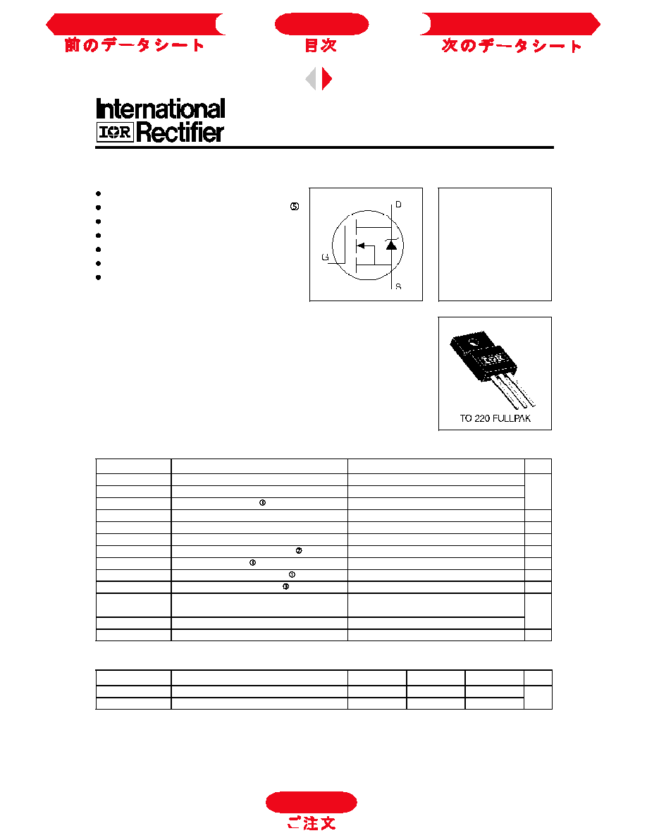
IRLI620G
HEXFET
Æ
Power MOSFET
PD - 9.1235
Revision 0
V
DSS
= 200V
R
DS(on)
= 0.80
I
D
= 4.0A
Absolute Maximum Ratings
Thermal Resistance
Parameter
Max.
Units
I
D
@ T
C
= 25∞C
Continuous Drain Current, V
GS
@ 5.0V
4.0
I
D
@ T
C
= 100∞C
Continuous Drain Current, V
GS
@ 5.0V
2.6
A
I
DM
Pulsed Drain Current
16
P
D
@T
C
= 25∞C
Power Dissipation
30
W
Linear Derating Factor
0.24
W/∞C
V
GS
Gate-to-Source Voltage
±10
V
E
AS
Single Pulse Avalanche Energy
62
mJ
I
AR
Avalanche Current
4.0
A
E
AR
Repetitive Avalanche Energy
3.0
mJ
dv/dt
Peak Diode Recovery dv/dt
5.0
V/ns
T
J
Operating Junction and
-55 to + 150
T
STG
Storage Temperature Range
∞C
Soldering Temperature, for 10 seconds
300 (1.6mm from case)
Mounting torque, 6-32 or M3 screw.
10 lbf∑in (1.1N∑m)
Isolated Package
High Voltage Isolation = 2.5KVRMS
Sink to Lead Creepage Dist. 4.8mm
Logic-Level Gate Drive
R
DS(ON)
Specified at V
GS
= 4V & 5V
Fast Switching
Ease of paralleling
Third Generation HEXFETs from International Rectifier provide the designer
with the best combination of fast switching, ruggedized device design, low on-
resistance and cost-effectiveness.
The TO-220 Fullpak eliminates the need for additional insulating hardware in
commercial-industrial applications. The moulding compound used provides a
high isolation capability and a low thermal resistance between the tab and external
heatsink. This isolation is equivalent to using a 100 micron mica barrier with
standard TO-220 product. The Fullpak is mounted to a heatsink using a single clip
or by a single screw fixing.
Description
∞C/W
Next Data Sheet
Index
Previous Datasheet
To Order
IRLI620G
Notes:
Parameter
Min. Typ. Max. Units
Conditions
I
S
Continuous Source Current
MOSFET symbol
(Body Diode)
showing the
I
SM
Pulsed Source Current
integral reverse
(Body Diode)
p-n junction diode.
V
SD
Diode Forward Voltage
≠≠≠
≠≠≠
1.8
V
T
J
= 25∞C, I
S
= 4.0A, V
GS
= 0V
t
rr
Reverse Recovery Time
≠≠≠
180
270
ns
T
J
= 25∞C, I
F
= 5.2A
Q
rr
Reverse RecoveryCharge
≠≠≠
1.1
1.7
µC
di/dt = 100A/µs
t
on
Forward Turn-On Time
Repetitive rating; pulse width limited by
max. junction temperature. ( See fig. 11 )
V
DD
= 25V, starting T
J
= 25∞C, L = 5.8mH
R
G
= 25
, I
AS
= 4.0A. (See Figure 12)
I
SD
5.2A, di/dt
95A/µs, V
DD
V
(BR)DSS
,
T
J
150∞C
Pulse width
300µs; duty cycle
2%.
Source-Drain Ratings and Characteristics
Electrical Characteristics @ T
J
= 25∞C (unless otherwise specified)
Parameter
Min. Typ. Max. Units
Conditions
V
(BR)DSS
Drain-to-Source Breakdown Voltage
200
≠≠≠
≠≠≠
V
V
GS
= 0V, ID = 250µA
V
(BR)DSS
/
T
J
Breakdown Voltage Temp. Coefficient
≠≠≠ 0.27 ≠≠≠
V/∞C Reference to 25∞C, I
D
= 1mA
≠≠≠
≠≠≠ 0.80
V
GS
= 5.0V, I
D
= 2.4A
≠≠≠
≠≠≠
1.0
V
GS
= 4.0V, I
D
= 2.0A
V
GS(th)
Gate Threshold Voltage
1.0
≠≠≠
2.0
V
V
DS
= V
GS
, I
D
= 250µA
g
fs
Forward Transconductance
1.2
≠≠≠
≠≠≠
S
V
DS
= 50V, I
D
= 3.1A
≠≠≠
≠≠≠
25
V
DS
= 200V, V
GS
= 0V
≠≠≠
≠≠≠
250
V
DS
= 160V, V
GS
= 0V, T
J
= 125∞C
Gate-to-Source Forward Leakage
≠≠≠
≠≠≠
100
V
GS
= 10V
Gate-to-Source Reverse Leakage
≠≠≠
≠≠≠ -100
V
GS
= -10V
Q
g
Total Gate Charge
≠≠≠
≠≠≠
16
I
D
= 5.2A
Q
gs
Gate-to-Source Charge
≠≠≠
≠≠≠
2.7
nC
V
DS
= 160V
Q
gd
Gate-to-Drain ("Miller") Charge
≠≠≠
≠≠≠
9.6
V
GS
= 10V, See Fig. 6 and 13
t
d(on)
Turn-On Delay Time
≠≠≠
4.2
≠≠≠
V
DD
= 100V
t
r
Rise Time
≠≠≠
31
≠≠≠
I
D
= 5.2A
t
d(off)
Turn-Off Delay Time
≠≠≠
18
≠≠≠
R
G
= 9.0
t
f
Fall Time
≠≠≠
17
≠≠≠
R
D
= 20
,
See Fig. 10
Between lead,
6mm (0.25in.)
from package
and center of die contact
C
iss
Input Capacitance
≠≠≠
360
≠≠≠
V
GS
= 0V
C
oss
Output Capacitance
≠≠≠
91
≠≠≠
pF
V
DS
= 25V
C
rss
Reverse Transfer Capacitance
≠≠≠
27
≠≠≠
= 1.0MHz, See Fig. 5
Intrinsic turn-on time is negligible (turn-on is dominated by L
S
+L
D
)
≠≠≠
≠≠≠
16
≠≠≠
≠≠≠
4.0
A
ns
I
DSS
Drain-to-Source Leakage Current
I
GSS
L
D
Internal Drain Inductance
≠≠≠
4.5
≠≠≠
L
S
Internal Source Inductance
≠≠≠
7.5
≠≠≠
nH
nA
µA
R
DS(ON)
Static Drain-to-Source On-Resistance
t=60s, =60Hz
Next Data Sheet
Index
Previous Datasheet
To Order

Fig 3. Typical Transfer Characteristics
Fig 4. Normalized On-Resistance
Vs. Temperature
IRLI620G
Fig 1. Typical Output Characteristics,
T
C
= 25
o
C
Fig 2. Typical Output Characteristics,
T
C
= 150
o
C
0.01
0.1
1
10
100
0.01
0.1
1
10
100
I
,
D
r
a
i
n
-
t
o
-
S
o
u
r
c
e
C
u
r
r
e
n
t
(
A
)
D
V , Drain-to-Source Voltage (V)
DS
VGS
TOP 7.50V
5.00V
4.00V
3.50V
3.00V
2.75V
2.50V
BOTTOM 2.25V
2.25V
20µs PULSE WIDTH
T = 150∞C
C
A
0.1
1
10
100
0.1
1
10
100
I
,
D
r
a
i
n
-
t
o
-
S
o
u
r
c
e
C
u
r
r
e
n
t
(
A
)
D
V , Drain-to-Source Voltage (V)
DS
VGS
TOP 7.50V
5.00V
4.00V
3.50V
3.00V
2.75V
2.50V
BOTTOM 2.25V
2.25V
20µs PULSE WIDTH
T = 150∞C
C
A
0.01
0.1
1
10
100
2.0
2.5
3.0
3.5
4.0
4.5
5.0
T = 25∞C
T = 150∞C
J
J
GS
V , Gate-to-Source Voltage (V)
D
I
,
D
r
a
i
n
-
t
o
-
S
o
u
r
c
e
C
u
r
r
e
n
t
(
A
)
V = 50V
20µs PULSE WIDTH
DS
A
0.0
0.5
1.0
1.5
2.0
2.5
-60 -40 -20
0
20
40
60
80 100 120 140 160
J
T , Junction Temperature (∞C)
R
,
D
r
a
i
n
-
t
o
-
S
o
u
r
c
e
O
n
R
e
s
i
s
t
a
n
c
e
D
S
(
o
n
)
(
N
o
r
m
a
l
i
z
e
d
)
V = 5.0V
GS
I = 5.2A
D
A
To Order
Next Data Sheet
Index
Previous Datasheet

IRLI620G
Fig 7. Typical Source-Drain Diode
Forward Voltage
Fig 8. Maximum Safe Operating Area
Fig 5. Typical Capacitance Vs.
Drain-to-Source Voltage
Fig 6. Typical Gate Charge Vs.
Gate-to-Source Voltage
0
500
1000
1500
2000
1
10
100
C
,
C
a
p
a
c
i
t
a
n
c
e
(
p
F
)
DS
V , Drain-to-Source Voltage (V)
A
V = 0V, f = 1MHz
C = C + C , C SHORTED
C = C
C = C + C
GS
iss gs gd ds
rss gd
oss ds gd
C
iss
C
oss
C
rss
0
2
4
6
8
10
0
4
8
12
16
Q , Total Gate Charge (nC)
G
FOR TEST CIRCUIT
SEE FIGURE 13
V
,
G
a
t
e
-
t
o
-
S
o
u
r
c
e
V
o
l
t
a
g
e
(
V
)
G
S
I = 5.2A
V = 160V
V = 100V
V = 40V
DS
DS
DS
D
A
0.1
1
10
100
0.3
0.6
0.9
1.2
1.5
T = 25∞C
T = 150∞C
J
J
V = 0V
GS
V , Source-to-Drain Voltage (V)
I
,
R
e
v
e
r
s
e
D
r
a
i
n
C
u
r
r
e
n
t
(
A
)
SD
S
D
A
0 .1
1
10
1 00
1
1 0
1 0 0
10 0 0
V , Drain-to-Source Voltage (V)
DS
I
,
D
r
a
i
n
C
u
r
r
e
n
t
(
A
)
OPERATION IN THIS AREA LIMITED
BY R
D
DS(on)
T = 25∞C
T = 150∞C
Single Pulse
C
J
100µs
1ms
10ms
100ms
A
To Order
Next Data Sheet
Index
Previous Datasheet

IRLI620G
Fig 10a. Switching Time Test Circuit
V
DS
5.0 V
Pulse Width
1
µs
Duty Factor
0.1 %
Fig 9. Maximum Drain Current Vs.
Case Temperature
Fig 10b. Switching Time Waveforms
R
D
V
GS
V
DD
R
G
D.U.T.
Fig 11. Maximum Effective Transient Thermal Impedance, Junction-to-Case
0.01
0.1
1
10
0.00001
0.0001
0.001
0.01
0.1
1
10
t , Rectangular Pulse Duration (sec)
1
t
h
J
C
D = 0 .5 0
0 .0 1
0 .0 2
0 .0 5
0 .1 0
0 .2 0
S IN G L E P UL S E
(T H E R M A L R E S P O N S E )
T
h
e
r
m
a
l
R
e
s
p
o
n
s
e
(
Z
)
A
P
t
2
1
t
D M
N o te s :
1 . D u ty fa c to r D = t / t
2 . P e a k T = P x Z + T
1
2
J
D M
th J C
C
0.0
1.0
2.0
3.0
4.0
25
50
75
100
125
150
C
I
,
D
r
a
i
n
C
u
r
r
e
n
t
(
A
m
p
s
)
D
T , Case Temperature (∞C)
A
To Order
Next Data Sheet
Index
Previous Datasheet