 | ÐлекÑÑоннÑй компоненÑ: IRLL014 | СкаÑаÑÑ:  PDF PDF  ZIP ZIP |
irll014n.p65
IRLL014N
HEXFET
®
Power MOSFET
S
D
G
V
DSS
= 55V
R
DS(on)
= 0.14
I
D
= 2.0A
Fifth Generation HEXFETs from International Rectifier
utilize advanced processing techniques to achieve
extremely low on-resistance per silicon area. This benefit,
combined with the fast switching speed and ruggedized
device design that HEXFET Power MOSFETs are well
known for, provides the designer with an extremely efficient
and reliable device for use in a wide variety of applications.
The SOT-223 package is designed for surface-mount
using vapor phase, infra red, or wave soldering techniques.
Its unique package design allows for easy automatic pick-
and-place as with other SOT or SOIC packages but has
the added advantage of improved thermal performance
due to an enlarged tab for heatsinking. Power dissipation
of 1.0W is possible in a typical surface mount application.
1/25/99
Description
l
Surface Mount
l
Advanced Process Technology
l
Ultra Low On-Resistance
l
Dynamic dv/dt Rating
l
Fast Switching
l
Fully Avalanche Rated
S O T -2 2 3
* When mounted on FR-4 board using minimum recommended footprint.
** When mounted on 1 inch square copper board, for comparison with other SMD devices.
Parameter
Typ.
Max.
Units
R
JA
Junction-to-Amb. (PCB Mount, steady state)*
90
120
R
JA
Junction-to-Amb. (PCB Mount, steady state)**
50
60
Thermal Resistance
°C/W
Parameter
Max.
Units
I
D
@ T
A
= 25°C
Continuous Drain Current, V
GS
@ 10V**
2.8
I
D
@ T
A
= 25°C
Continuous Drain Current, V
GS
@ 10V*
2.0
I
D
@ T
A
= 70°C
Continuous Drain Current, V
GS
@ 10V*
1.6
I
DM
Pulsed Drain Current
16
P
D
@T
A
= 25°C
Power Dissipation (PCB Mount)**
2.1
W
P
D
@T
A
= 25°C
Power Dissipation (PCB Mount)*
1.0
W
Linear Derating Factor (PCB Mount)*
8.3
mW/°C
V
GS
Gate-to-Source Voltage
± 16
V
E
AS
Single Pulse Avalanche Energy
32
mJ
I
AR
Avalanche Current
2.0
A
E
AR
Repetitive Avalanche Energy
*
0.1
mJ
dv/dt
Peak Diode Recovery dv/dt
7.2
V/ns
T
J,
T
STG
Junction and Storage Temperature Range
-55 to + 150
°C
Absolute Maximum Ratings
A
PD- 91499B
www.irf.com
1
IRLL014N
2
www.irf.com
Parameter
Min. Typ. Max. Units
Conditions
V
(BR)DSS
Drain-to-Source Breakdown Voltage
55
V
V
GS
= 0V, I
D
= 250µA
V
(BR)DSS
/
T
J
Breakdown Voltage Temp. Coefficient
0.015
V/°C
Reference to 25°C, I
D
= 1mA
0.14
V
GS
= 10V, I
D
= 2.0A
0.20
V
GS
= 5.0V, I
D
= 1.2A
0.28
V
GS
= 4.0V, I
D
= 1.0A
V
GS(th)
Gate Threshold Voltage
1.0
2.0
V
V
DS
= V
GS
, I
D
= 250µA
g
fs
Forward Transconductance
2.3
S
V
DS
= 25V, I
D
= 1.0A
25
µA
V
DS
= 55V, V
GS
= 0V
250
V
DS
= 44V, V
GS
= 0V, T
J
= 150°C
Gate-to-Source Forward Leakage
100
nA
V
GS
= 16V
Gate-to-Source Reverse Leakage
-100
V
GS
= -16V
Q
g
Total Gate Charge
9.5
14
I
D
= 2.0A
Q
gs
Gate-to-Source Charge
1.1
1.7
nC
V
DS
= 44V
Q
gd
Gate-to-Drain ("Miller") Charge
3.0
4.4
V
GS
= 10V, See Fig. 6 and 9
t
d(on)
Turn-On Delay Time
5.1
V
DD
= 28V
t
r
Rise Time
4.9
ns
I
D
= 2.0A
t
d(off)
Turn-Off Delay Time
14
R
G
= 6.0
t
f
Fall Time
2.9
R
D
= 14
,
See Fig. 10
C
iss
Input Capacitance
230
V
GS
= 0V
C
oss
Output Capacitance
66
pF
V
DS
= 25V
C
rss
Reverse Transfer Capacitance
30
= 1.0MHz, See Fig. 5
Electrical Characteristics @ T
J
= 25°C (unless otherwise specified)
I
GSS
R
DS(on)
Static Drain-to-Source On-Resistance
I
DSS
Drain-to-Source Leakage Current
Repetitive rating; pulse width limited by
max. junction temperature. ( See fig. 11 )
I
SD
2.0A, di/dt
170A/µs, V
DD
V
(BR)DSS
,
T
J
150°C
Notes:
V
DD
= 25V, starting T
J
= 25°C, L = 4.0mH
R
G
= 25
, I
AS
= 4.0A. (See Figure 12)
Pulse width
300µs; duty cycle
2%.
Parameter
Min. Typ. Max. Units
Conditions
I
S
Continuous Source Current
MOSFET symbol
(Body Diode)
showing the
I
SM
Pulsed Source Current
integral reverse
(Body Diode)
p-n junction diode.
V
SD
Diode Forward Voltage
1.0
V
T
J
= 25°C, I
S
= 2.0A, V
GS
= 0V
t
rr
Reverse Recovery Time
41
61
ns
T
J
= 25°C, I
F
= 2.0A
Q
rr
Reverse RecoveryCharge
73
110
nC
di/dt = 100A/µs
t
on
Forward Turn-On Time
Intrinsic turn-on time is negligible (turn-on is dominated by L
S
+L
D
)
Source-Drain Ratings and Characteristics
16
1.3
A
IRLL014N
www.irf.com
3
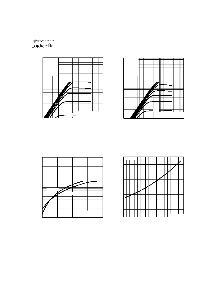
Fig 3. Typical Transfer Characteristics
Fig 4. Normalized On-Resistance
Vs. Temperature
Fig 1. Typical Output Characteristics,
Fig 2. Typical Output Characteristics,
1
1 0
1 0 0
0 . 1
1
1 0
1 0 0
20 µ s P U LS E W ID TH
T = 2 5°C
A
J
D S
V , D ra in -to -S o urc e V o ltag e (V )
3.0V
VGS
TO P 15V
10V
7.0V
5.5V
4.5V
4.0V
3.5V
BOT TOM 3.0V
DI
,
D
r
ai
n-
t
o
-
S
o
u
r
c
e C
u
r
r
ent
(
A
)
1
1 0
1 0 0
0 . 1
1
1 0
1 0 0
A
D S
V , D rain-to-S ource V oltage (V )
DI
,
D
r
a
i
n-
t
o
-
S
our
c
e
C
u
r
r
en
t
(
A
)
2 0µ s P U L S E W ID T H
T = 15 0°C
J
3.0 V
VGS
TOP 15V
10V
7.0V
5.5V
4.5V
4.0V
3.5V
BOTTOM 3.0V
1
1 0
1 0 0
3 . 0
4 . 0
5 . 0
6 . 0
7 . 0
T = 25 °C
T = 1 50 °C
J
J
G S
V , G ate-to -S o urce V oltag e (V )
D
I
,
D
r
a
i
n
-
t
o
-
S
o
u
rc
e
C
u
rre
n
t
(A
)
A
V = 2 5 V
2 0 µ s P UL S E W ID TH
D S
0 . 0
0 . 5
1 . 0
1 . 5
2 . 0
- 6 0
- 4 0
- 2 0
0
2 0
4 0
6 0
8 0
1 0 0
1 2 0
1 4 0
1 6 0
J
T , J unc tion T em perature (°C )
R
, D
r
a
i
n
-
to
-
S
o
u
r
c
e
O
n
R
e
s
i
s
t
a
n
c
e
D
S
(
on)
(N
o
r
m
a
li
z
e
d
)
V = 1 0V
G S
A
I = 2.0 A
D
IRLL014N
4
www.irf.com
Fig 8. Maximum Safe Operating Area
Fig 6. Typical Gate Charge Vs.
Gate-to-Source Voltage
Fig 5. Typical Capacitance Vs.
Drain-to-Source Voltage
Fig 7. Typical Source-Drain Diode
Forward Voltage
0
1 0 0
2 0 0
3 0 0
4 0 0
1
1 0
1 0 0
C
,
Cap
ac
i
t
a
n
c
e
(
p
F
)
D S
V , D rain-to-S ourc e V oltage (V )
A
V = 0V , f = 1M H z
C = C + C , C S H O R T E D
C = C
C = C + C
G S
is s g s g d d s
rs s g d
o ss d s gd
C
iss
C
os s
C
rs s
0
4
8
1 2
1 6
2 0
0
3
6
9
1 2
1 5
Q , T otal G ate C harge (nC )
G
V
, G
a
te
-
t
o
-
S
o
u
r
c
e
V
o
l
t
a
g
e
(
V
)
GS
A
F O R TE S T C IR C U IT
S E E F IG U R E 9
I = 2.0 A
V = 4 4V
V = 2 8V
D
D S
D S
0 . 1
1
1 0
1 0 0
0 . 4
0 . 6
0 . 8
1 . 0
1 . 2
1 . 4
1 . 6
T = 2 5°C
T = 1 50 °C
J
J
V = 0V
G S
V , S o urc e-to -D ra in V o lta ge (V )
I , R
e
v
e
r
s
e
D
r
a
i
n
C
u
r
r
e
n
t
(
A
)
S D
SD
A
0.1
1
1 0
1 0 0
1
1 0
1 0 0
V , D ra in-to-S o u rce V o lta ge (V )
D S
I , D
r
a
i
n
C
u
r
r
e
n
t
(
A
)
O P E R A T IO N IN T H IS A R E A L IM ITE D
B Y R
D
D S (o n)
T = 25 °C
T = 15 0°C
S ing le P u ls e
1 0 µ s
1 0 0 µ s
1 m s
1 0 m s
A
A
J
IRLL014N
www.irf.com
5
Q
G
Q
GS
Q
GD
V
G
Charge
+
-
V
DS
10V
Pulse Width
1
µs
Duty Factor
0.1 %
R
D
V
GS
V
DD
R
G
D.U.T.
D.U.T.
V
DS
I
D
I
G
3mA
V
GS
.3
µ
F
50K
.2
µ
F
12V
Current Regulator
Same Type as D.U.T.
Current Sampling Resistors
+
-
V
DS
90%
10%
V
GS
t
d(on)
t
r
t
d(off)
t
f
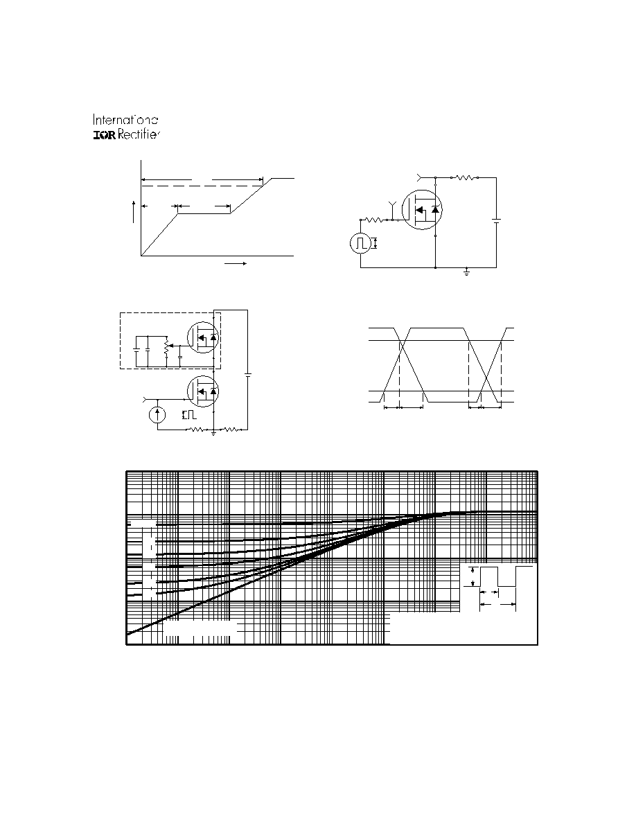
Fig 10b. Switching Time Waveforms
Fig 10a. Switching Time Test Circuit
Fig 9a. Basic Gate Charge Waveform
Fig 9b. Gate Charge Test Circuit
Fig 11. Maximum Effective Transient Thermal Impedance, Junction-to-Ambient
10V
0 . 1
1
1 0
1 0 0
1 0 0 0
0 . 0 0 0 0 1
0 . 0 0 0 1
0 . 0 0 1
0 . 0 1
0 . 1
1
1 0
1 0 0
1 0 0 0
t , R e cta n g u lar P u lse D u ra tio n (se c )
1
D = 0.5 0
0 .0 1
0 .0 2
0 .0 5
0 .1 0
0 .2 0
S IN G L E P U L S E
( T H E R M A L R E S P O N S E )
A
T
her
m
a
l
R
e
s
pons
e (
Z
)
th
J
A
P
t 2
1
t
D M
N ote s:
1 . D u ty fac to r D = t / t
2 . P e a k T = P x Z + T
1
2
J
D M
th J A
A