 | –≠–ª–µ–∫—Ç—Ä–æ–Ω–Ω—ã–π –∫–æ–º–ø–æ–Ω–µ–Ω—Ç: IRLMS6702 | –°–∫–∞—á–∞—Ç—å:  PDF PDF  ZIP ZIP |

IRLMS6702
V
DSS
= -20V
R
DS(on)
= 0.20
HEXFET
Æ
Power MOSFET
Fifth Generation HEXFET
Æ
power MOSFETs from
International Rectifier utilize advanced processing
techniques to achieve extremely low on-resistance
per silicon area. This benefit, combined with the fast
switching speed and ruggedized device design that
HEXFET
Æ
power MOSFETs are well known for,
provides the designer with an extremely efficient and
reliable device for use in a wide variety of applications.
The Micro6
package with its customized leadframe
produces a HEXFET
Æ
power MOSFET with R
DS(on)
60% less than a similar size SOT-23. This package is
ideal for applications where printed circuit board space
is at a premium. It's unique thermal design and R
DS(on)
reduction enables a current-handling increase of
nearly 300% compared to the SOT-23.
Description
3/18/04
l
Generation V Technology
l
Micro6 Package Style
l
Ultra Low
R
DS(on)
l
P-Channel MOSFET
Absolute Maximum Ratings
Parameter
Max.
Units
I
D
@ T
A
= 25∞C
Continuous Drain Current, V
GS
@ -4.5V
-2.4
I
D
@ T
A
= 70∞C
Continuous Drain Current, V
GS
@ -4.5V
-1.9
A
I
DM
Pulsed Drain Current
-13
P
D
@T
A
= 25∞C
Power Dissipation
1.7
W
Linear Derating Factor
13
mW/∞C
V
GS
Gate-to-Source Voltage
± 12
V
dv/dt
Peak Diode Recovery dv/dt
5.0
V/ns
T
J,
T
STG
Junction and Storage Temperature Range
-55 to + 150
∞C
Top View
1
2
D
G
A
D
D
D
S
3
4
5
6
Parameter Min. Typ. Max Units
R
JA
Maximum Junction-to-Ambient
75 ∞C/W
Thermal Resistance Ratings
www.irf.com
1
Micro6
PD - 91414C
IRLMS6702
2
www.irf.com
Parameter
Min. Typ. Max. Units
Conditions
V
(BR)DSS
Drain-to-Source Breakdown Voltage
-20
V
V
GS
= 0V, I
D
= -250µA
V
(BR)DSS
/T
J
Breakdown Voltage Temp. Coefficient
-0.005
V/∞C Reference to 25∞C, I
D
= -1mA
0.200
V
GS
= -4.5V, I
D
= -1.6A
0.375
V
GS
= -2.7V, I
D
= -0.80A
V
GS(th)
Gate Threshold Voltage
-0.70
V
V
DS
= V
GS
, I
D
= -250µA
g
fs
Forward Transconductance
1.5
S
V
DS
= -10V, I
D
= -0.80A
-1.0
V
DS
= -16V, V
GS
= 0V
-25
V
DS
= -16V, V
GS
= 0V, T
J
= 125∞C
Gate-to-Source Forward Leakage
-100
V
GS
= -12V
Gate-to-Source Reverse Leakage
100
V
GS
= 12V
Q
g
Total Gate Charge
5.8
8.8
I
D
= -1.6A
Q
gs
Gate-to-Source Charge
1.8
2.6
nC
V
DS
= -16V
Q
gd
Gate-to-Drain ("Miller") Charge
2.1
3.1
V
GS
= -4.5V, See Fig. 6 and 9
t
d(on)
Turn-On Delay Time
13
V
DD
= -10V
t
r
Rise Time
20
I
D
= -1.6A
t
d(off)
Turn-Off Delay Time
21
R
G
= 6.0
t
f
Fall Time
18
R
D
= 6.1, See Fig. 10
C
iss
Input Capacitance
210
V
GS
= 0V
C
oss
Output Capacitance
130
pF
V
DS
= -15V
C
rss
Reverse Transfer Capacitance
73
= 1.0MHz, See Fig. 5
Electrical Characteristics @ T
J
= 25∞C (unless otherwise specified)
I
GSS
µA
R
DS(on)
Static Drain-to-Source On-Resistance
I
DSS
Drain-to-Source Leakage Current
nA
ns
Parameter
Min. Typ. Max. Units
Conditions
I
S
Continuous Source Current
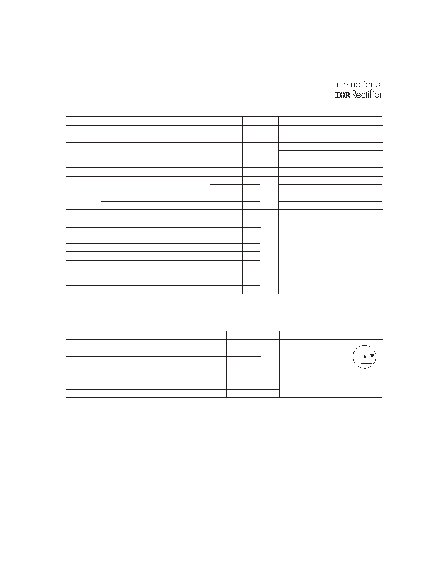
MOSFET symbol
(Body Diode)
showing the
I
SM
Pulsed Source Current
integral reverse
(Body Diode)
p-n junction diode.
V
SD
Diode Forward Voltage
-1.2
V
T
J
= 25∞C, I
S
= -1.6A, V
GS
= 0V
t
rr
Reverse Recovery Time
25
37
ns
T
J
= 25∞C, I
F
= -1.6A
Q
rr
Reverse RecoveryCharge
15
22
nC
di/dt = -100A/µs
Source-Drain Ratings and Characteristics
A
-13
-1.7
S
D
G
Repetitive rating; pulse width limited by
max. junction temperature. ( See fig. 11 )
I
SD
-1.6A, di/dt -100A/µs, V
DD
V
(BR)DSS
,
T
J
150∞C
Notes:
Pulse width 300µs; duty cycle 2%.
Surface mounted on FR-4 board, t 5sec.

IRLMS6702
www.irf.com
3
Fig 3. Typical Transfer Characteristics
Fig 4. Normalized On-Resistance
Vs. Temperature
Fig 2. Typical Output Characteristics
Fig 1. Typical Output Characteristics
0.1
1
10
100
0.1
1
10
D
DS
20µs PULSE WIDTH
T = 25∞C
A
-I , D
r
a
i
n
-
to
-
S
o
u
rc
e
C
u
rr
e
n
t (A
)
-V , Drain-to-Source Voltage (V)
J
-1.75V
VGS
TOP - 7.5V
- 5.0V
- 4.0V
- 3.5V
- 3.0V
- 2.5V
- 2.0V
BOTTOM -1.75V
0.1
1
10
100
0.1
1
10
D
DS
20µs PULSE WIDTH
T = 150∞C
A
-I , D
r
a
i
n
-
to
-S
o
u
rce
C
u
rren
t
(A
)
-V , Drain-to-Source Voltage (V)
J
-1.75V
VGS
TOP - 7.5V
- 5.0V
- 4.0V
- 3.5V
- 3.0V
- 2.5V
- 2.0V
BOTTOM -1.75V
0.1
1
10
100
1.5
2.0
2.5
3.0
3.5
4.0
4.5
5.0
T = 25∞C
T = 150∞C
J
J
GS
D
A
-I
,
Dra
i
n
-
t
o
-S
o
u
rc
e
C
u
rre
n
t
(A)
-V , Gate-to-Source Voltage (V)
V = -10V
20µs PULSE WIDTH
DS
0.0
0.5
1.0
1.5
2.0
-60
-40
-20
0
20
40
60
80
100 120 140 160
J
T , Junction Temperature (∞C)
R
, D
r
a
i
n
-
to
-
S
o
u
rc
e
O
n
R
e
s
i
s
t
a
n
c
e
DS
(
on)
(N
o
r
m
a
l
i
ze
d)
A
I = -1.6A
V = -4.5V
D
GS

IRLMS6702
4
www.irf.com
Fig 8. Maximum Safe Operating Area
Fig 6. Typical Gate Charge Vs.
Gate-to-Source Voltage
Fig 5. Typical Capacitance Vs.
Drain-to-Source Voltage
Fig 7. Typical Source-Drain Diode
Forward Voltage
0
100
200
300
400
1
10
100
C
,
C
a
p
a
c
i
ta
n
c
e
(p
F
)
A
DS
-V , Drain-to-Source Voltage (V)
V = 0V, f = 1MHz
C = C + C , C SHORTED
C = C
C = C + C
GS
iss gs gd ds
rss gd
oss ds gd
C
iss
C
oss
C
rss
0
2
4
6
8
10
0
2
4
6
8
10
G
GS
A
-V
, G
a
te
-to
-
S
o
u
r
c
e
V
o
lta
g
e
(V
)
Q , Total Gate Charge (nC)
I = -1.6A
V = -16V
FOR TEST CIRCUIT
SEE FIGURE 9
D
DS
0.1
1
10
100
0.4
0.6
0.8
1.0
1.2
1.4
T = 25∞C
T = 150∞C
J
J
V = 0V
GS
SD
SD
A
-
I
, R
e
v
e
rs
e
D
r
a
i
n
C
u
rre
n
t
(
A
)
-V , Source-to-Drain Voltage (V)
0.1
1
10
100
1
10
100
OPERATION IN THIS AREA LIMITED
BY R
DS(on)
T = 25∞C
T = 150∞C
Single Pulse
A
-I , D
r
a
i
n C
u
rre
nt (A
)
-V , Drain-to-Source Voltage (V)
DS
D
A
J
100µs
1ms
10ms

IRLMS6702
www.irf.com
5
Fig 10b. Switching Time Waveforms
Fig 10a. Switching Time Test Circuit
Fig 9a. Basic Gate Charge Waveform
Fig 9b. Gate Charge Test Circuit
V
DS
-4.5V
Pulse Width 1 µs
Duty Factor 0.1 %
R
D
V
GS
V
DD
R
G
D.U.T.
+
-
Q
G
Q
GS
Q
GD
V
G
Charge
-4.5V
V
DS
90%
10%
V
GS
t
d(on)
t
r
t
d(off)
t
f
D.U.T.
V
DS
I
D
I
G
-3mA
V
GS
.3
µ
F
50K
.2
µ
F
12V
Current Regulator
Same Type as D.U.T.
Current Sampling Resistors
+
-
Fig 11. Maximum Effective Transient Thermal Impedance, Junction-to-Ambient
0.1
1
10
100
0.00001
0.0001
0.001
0.01
0.1
1
10
100
Notes:
1. Duty factor D = t / t
2. Peak T = P
x Z
+ T
1
2
J
DM
thJA
A
P
t
t
DM
1
2
t , Rectangular Pulse Duration (sec)
Ther
m
a
l
R
e
sponse
(
Z
)
1
th
J
A
0.01
0.02
0.05
0.10
0.20
D = 0.50
SINGLE PULSE
(THERMAL RESPONSE)