 | –≠–ª–µ–∫—Ç—Ä–æ–Ω–Ω—ã–π –∫–æ–º–ø–æ–Ω–µ–Ω—Ç: IRLR3103 | –°–∫–∞—á–∞—Ç—å:  PDF PDF  ZIP ZIP |
HEXFET
Æ
Power MOSFET
IRLR/U3103
PD - 9.1333B
l
Logic-Level Gate Drive
l
Ultra Low On-Resistance
l
Surface Mount (IRLR3103)
l
Straight Lead (IRLU3103)
l
Advanced Process Technology
l
Fast Switching
l
Fully Avalanche Rated
8/7/96
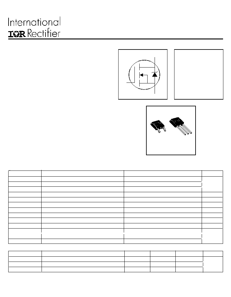
V
DSS
= 30V
R
DS(on)
= 0.019
I
D
= 46A
S
D
G
D - P A K
T O - 2 52 A A
I- P A K
TO - 2 5 1 A A
Fifth Generation HEXFETs from International Rectifier
utilize advanced processing techniques to achieve the
lowest possible on-resistance per silicon area. This benefit,
combined with the fast switching speed and ruggedized
device design that HEXFET Power MOSFETs are well
known for, provides the designer with an extremely efficient
device for use in a wide variety of applications.
The D-PAK is designed for surface mounting using vapor
phase, infrared, or wave soldering techniques. The straight
lead version (IRFU series) is for through-hole mounting
applications. Power dissipation levels up to 1.5 watts are
possible in typical surface mount applications.
Description
PRELIMINARY
Parameter
Max.
Units
I
D
@ T
C
= 25∞C
Continuous Drain Current, V
GS
@ 10V
46
I
D
@ T
C
= 100∞C
Continuous Drain Current, V
GS
@ 10V
29
A
I
DM
Pulsed Drain Current
220
P
D
@T
C
= 25∞C
Power Dissipation
69
W
Linear Derating Factor
0.56
W/∞C
V
GS
Gate-to-Source Voltage
±16
V
E
AS
Single Pulse Avalanche Energy
240
mJ
I
AR
Avalanche Current
34
A
E
AR
Repetitive Avalanche Energy
6.9
mJ
dv/dt
Peak Diode Recovery dv/dt
2.0
V/ns
T
J
Operating Junction and
-55 to + 150
T
STG
Storage Temperature Range
∞C
Soldering Temperature, for 10 seconds
300 (1.6mm from case)
Absolute Maximum Ratings
Parameter
Min.
Typ.
Max.
Units
R
JC
Junction-to-Case
≠≠≠≠
≠≠≠≠
1.8
R
JA
Junction-to-Ambient (PCB mount)**
≠≠≠≠
≠≠≠≠
50
∞C/W
R
JA
Junction-to-Ambient
≠≠≠≠
≠≠≠≠
110
Thermal Resistance
** When mounted on 1" square PCB (FR-4 or G-10 Material ) .
For recommended footprint and soldering techniques refer to application note #AN-994
IRLR/U3103
Parameter
Min. Typ. Max. Units
Conditions
V
(BR)DSS
Drain-to-Source Breakdown Voltage
30
≠≠≠
≠≠≠
V
V
GS
= 0V, I
D
= 250µA
V
(BR)DSS
/
T
J
Breakdown Voltage Temp. Coefficient
≠≠≠
0.037 ≠≠≠
V/∞C
Reference to 25∞C, I
D
= 1mA
≠≠≠
≠≠≠ 0.019
V
GS
= 10V, I
D
= 28A
≠≠≠
≠≠≠ 0.024
V
GS
= 4.5V, I
D
= 23A
V
GS(th)
Gate Threshold Voltage
1.0
≠≠≠
≠≠≠
V
V
DS
= V
GS
, I
D
= 250µA
g
fs
Forward Transconductance
23
≠≠≠
≠≠≠
S
V
DS
= 25V, I
D
= 34A
≠≠≠
≠≠≠
25
V
DS
= 30V, V
GS
= 0V
≠≠≠
≠≠≠
250
V
DS
= 24V, V
GS
= 0V, T
J
= 125∞C
Gate-to-Source Forward Leakage
≠≠≠
≠≠≠
100
V
GS
= 16V
Gate-to-Source Reverse Leakage
≠≠≠
≠≠≠
-100
V
GS
= -16V
Q
g
Total Gate Charge
≠≠≠
≠≠≠
50
I
D
= 34A
Q
gs
Gate-to-Source Charge
≠≠≠
≠≠≠
14
nC
V
DS
= 24V
Q
gd
Gate-to-Drain ("Miller") Charge
≠≠≠
≠≠≠
28
V
GS
= 4.5V, See Fig. 6 and 13
t
d(on)
Turn-On Delay Time
≠≠≠
9.0
≠≠≠
V
DD
= 15V
t
r
Rise Time
≠≠≠
210
≠≠≠
I
D
= 34A
t
d(off)
Turn-Off Delay Time
≠≠≠
20
≠≠≠
R
G
= 3.4
,
V
GS
= 4.5V
t
f
Fall Time
≠≠≠
54
≠≠≠
R
D
= 0.43
,
See Fig. 10
Between lead,
6mm (0.25in.)
from package
and center of die contact
C
iss
Input Capacitance
≠≠≠
1600 ≠≠≠
V
GS
= 0V
C
oss
Output Capacitance
≠≠≠
640
≠≠≠
pF
V
DS
= 25V
C
rss
Reverse Transfer Capacitance
≠≠≠
320
≠≠≠
= 1.0MHz, See Fig. 5
Electrical Characteristics @ T
J
= 25∞C (unless otherwise specified)
nA
S
D
G
I
DSS
Drain-to-Source Leakage Current
R
DS(on)
Static Drain-to-Source On-Resistance
I
GSS
L
D
Internal Drain Inductance
≠≠≠
4.5
≠≠≠
L
S
Internal Source Inductance
≠≠≠
7.5
≠≠≠
ns
µA
nH
Caculated continuous current based on maximum allowable junction temperature;
Package limitation current = 20A.
Repetitive rating; pulse width limited by
max. junction temperature. ( See fig. 11 )
This is applied for I-PAK, L
S
of D-PAK is measured between lead and center of
die contact
V
DD
= 15V, starting T
J
= 25∞C, L = 300µH
R
G
= 25
, I
AS
= 34A. (See Figure 12)
I
SD
34A, di/dt
140A/µs, V
DD
V
(BR)DSS
,
T
J
150∞C
Uses IRL3103 data and test conditions.
Pulse width
300µs; duty cycle
2%.
Parameter
Min. Typ. Max. Units
Conditions
I
S
Continuous Source Current
MOSFET symbol
(Body Diode)
showing the
I
SM
Pulsed Source Current
integral reverse
(Body Diode)
p-n junction diode.
V
SD
Diode Forward Voltage
≠≠≠
≠≠≠
1.3
V
T
J
= 25∞C, I
S
= 28A, V
GS
= 0V
t
rr
Reverse Recovery Time
≠≠≠
81
120
ns
T
J
= 25∞C, I
F
= 34A
Q
rr
Reverse RecoveryCharge
≠≠≠
210
310
nC
di/dt = 100A/µs
t
on
Forward Turn-On Time
Intrinsic turn-on time is negligible (turn-on is dominated by L
S
+L
D
)
A
≠≠≠
≠≠≠ 220
≠≠≠
≠≠≠
46
S
D
G
Source-Drain Ratings and Characteristics
Rev. #
Parameters Old spec.
New spec.
Comments
Revision Date
1
V
GS(th)
(Max.)
2.5V
No spec.
Removed V
GS(th)
Max. Specification
5/1/96
1
V
GS
(Max.)
±20
±16
Decrease V
GS
Max. Specification
5/1/96
Specification changes
Notes:
IRLR/U3103
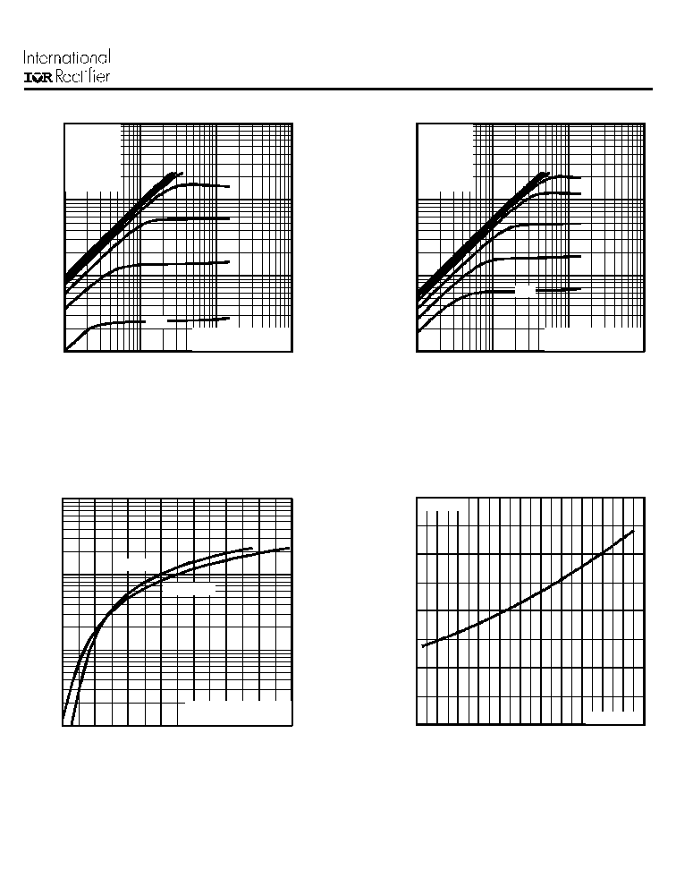
Fig 1. Typical Output Characteristics,
T
J
= 25
o
C
Fig 3. Typical Transfer Characteristics
Fig 4. Normalized On-Resistance
Vs. Temperature
Fig 2. Typical Output Characteristics,
T
J
= 150
o
C
1
1 0
1 0 0
1 0 0 0
0 . 1
1
1 0
1 0 0
I
, D
r
a
i
n
-
to
-
S
o
u
r
c
e
C
u
r
r
e
n
t
(
A
)
D
V , Drain -to -S o urce Vo lta ge (V )
D S
A
VGS
TOP 15V
12V
10V
8.0V
6.0V
4.0V
3.0V
BOTTOM 2.5V
2.5 V
2 0µ s PU L SE W ID TH
T = 1 50 ∞C
J
1
1 0
1 0 0
1 0 0 0
2 . 0
3 . 0
4 . 0
5 . 0
6 . 0
7 . 0
8 . 0
9 . 0
T = 2 5 ∞C
T = 1 5 0 ∞ C
J
J
G S
V , G a te -to -S o u rce V o lta ge (V )
D
I
, D
r
a
i
n
-
to
-
S
o
u
r
c
e
C
u
r
r
e
n
t
(
A
)
A
V = 1 5 V
2 0 µ s P U L S E W ID T H
DS
0 . 0
0 . 5
1 . 0
1 . 5
2 . 0
- 6 0
- 4 0
- 2 0
0
2 0
4 0
6 0
8 0
1 0 0
1 2 0
1 4 0
1 6 0
J
T , Ju nctio n T emp eratu re (∞C)
R
,
D
r
a
i
n
-
to
-
S
o
u
r
c
e
O
n
R
e
s
i
s
t
a
n
c
e
D
S
(
on)
(
N
o
r
m
a
l
i
z
ed)
V = 10 V
G S
A
I = 46 A
D
1
1 0
1 0 0
1 0 0 0
0 . 1
1
1 0
1 0 0
I
, D
r
a
i
n
-
to
-
S
o
u
r
c
e
C
u
r
r
e
n
t
(
A
)
D
V , Dra in-to-So urce V olta ge (V )
D S
A
20 µ s PU LSE W ID TH
T = 2 5∞C
J
VGS
TOP 15V
12V
10V
8.0V
6.0V
4.0V
3.0V
BOTT OM 2.5V
2.5 V
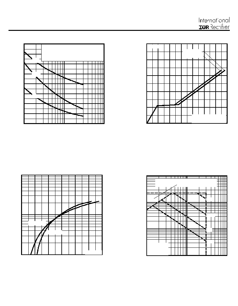
IRLR/U3103
Fig 7. Typical Source-Drain Diode
Forward Voltage
Fig 5. Typical Capacitance Vs.
Drain-to-Source Voltage
Fig 8. Maximum Safe Operating Area
Fig 6. Typical Gate Charge Vs.
Gate-to-Source Voltage
0
4 0 0
8 0 0
1 2 0 0
1 6 0 0
2 0 0 0
2 4 0 0
2 8 0 0
3 2 0 0
1
1 0
1 0 0
C
,
C
a
pac
i
t
anc
e (
p
F
)
D S
V , Drai n-to -So urce V oltag e (V)
A
V = 0V , f = 1MH z
C = C + C , C SH OR TED
C = C
C = C + C
G S
is s gs g d ds
rs s g d
os s ds gd
C
is s
C
o s s
C
rs s
0
3
6
9
1 2
1 5
0
1 0
2 0
3 0
4 0
5 0
6 0
7 0
Q , T otal Ga te C harg e (nC )
G
V
,
G
a
t
e
-
t
o-
S
o
u
r
c
e
V
o
l
t
ag
e (
V
)
GS
A
FO R TEST CI R CU I T
SEE FIG UR E 13
V = 2 4V
V = 1 5V
I = 34A
DS
DS
D
1 0
1 0 0
1 0 0 0
0 . 4
0 . 8
1 . 2
1 . 6
2 . 0
2 . 4
2 . 8
T = 25 ∞C
T = 15 0∞C
J
J
V = 0 V
G S
V , S o urce-to -Drain Vo lta ge (V )
I
, R
e
v
e
r
s
e
D
r
a
i
n
C
u
r
r
e
n
t
(
A
)
S D
SD
A
1
1 0
1 0 0
1 0 0 0
1
1 0
1 0 0
V , Dra in -to-So urce Vo ltag e (V)
D S
I
,
D
r
ai
n C
u
r
r
en
t
(
A
)
OPE R ATIO N IN TH IS A RE A LI MI TE D
BY R
D
D S(o n)
T = 25 ∞C
T = 15 0∞C
S ing le Pulse
C
J
10µ s
1 00µs
1m s
10m s
A
IRLR/U3103
Fig 9. Maximum Drain Current Vs.
Case Temperature
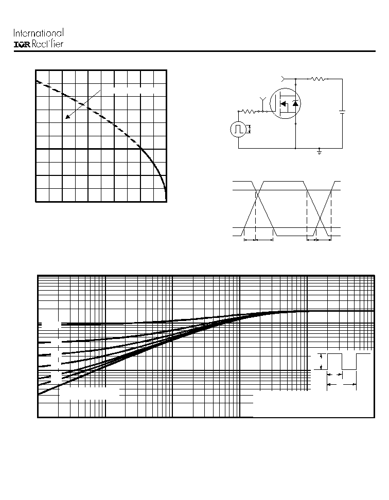
Fig 10a. Switching Time Test Circuit
V
DS
90%
10%
V
GS
t
d(on)
t
r
t
d(off)
t
f
Fig 10b. Switching Time Waveforms
Fig 11. Maximum Effective Transient Thermal Impedance, Junction-to-Case
V
DS
Pulse Width
1
µs
Duty Factor
0.1 %
R
D
V
GS
R
G
D.U.T.
4.5V
+
-
V
DD
0
1 0
2 0
3 0
4 0
5 0
2 5
5 0
7 5
1 0 0
1 2 5
1 5 0
C
I
,
D
r
ai
n
C
u
r
r
ent
(
A
m
p
s
)
D
T , Ca se Te mpe ra ture (∞C )
A
L IM IT E D B Y P A C K A G E
0 . 0 1
0 . 1
1
1 0
0 . 0 0 0 0 1
0 . 0 0 0 1
0 . 0 0 1
0 . 0 1
0 . 1
1
t , Rectan gular Pulse Duration (sec)
1
th
J
C
D = 0.50
0 .0 1
0 .0 2
0 .0 5
0 .1 0
0 .2 0
S IN G L E P U L S E
(T HE RM A L R E S P O NS E )
A
Ther
m
a
l
R
e
sp
onse (
Z
)
P
t
2
1
t
D M
N o te s :
1 . D u ty fa c to r D = t / t
2. P e a k T = P x Z + T
1
2
J
DM
t h J C
C