 | ÐлекÑÑоннÑй компоненÑ: IRLR7821 | СкаÑаÑÑ:  PDF PDF  ZIP ZIP |
Äîêóìåíòàöèÿ è îïèñàíèÿ www.docs.chipfind.ru
www.irf.com
1
4/5/04
IRLR7821
IRLU7821
HEXFET
®
Power MOSFET
Notes
through
are on page 11
Applications
Benefits
l
Very Low RDS(on) at 4.5V V
GS
l
Ultra-Low Gate Impedance
l
Fully Characterized Avalanche Voltage
and Current
l
High Frequency Synchronous Buck
Converters for Computer Processor Power
l
High Frequency Isolated DC-DC
Converters with Synchronous Rectification
for Telecom and Industrial Use
D-Pak
IRLR7821
I-Pak
IRLU7821
V
DSS
R
DS(on)
max
Qg
30V
10m
:
10nC
PD - 94538B
Absolute Maximum Ratings
Parameter
Units
V
DS
Drain-to-Source Voltage
V
V
GS
Gate-to-Source Voltage
I
D
@ T
C
= 25°C
Continuous Drain Current, V
GS
@ 10V
I
D
@ T
C
= 100°C
Continuous Drain Current, V
GS
@ 10V
A
I
DM
Pulsed Drain Current
P
D
@T
C
= 25°C
Maximum Power Dissipation
g
W
P
D
@T
C
= 100°C
Maximum Power Dissipation
g
Linear Derating Factor
W/°C
T
J
Operating Junction and
°C
T
STG
Storage Temperature Range
Thermal Resistance
Parameter
Typ.
Max.
Units
R
JC
Junction-to-Case
2.0
R
JA
Junction-to-Ambient (PCB Mount)
gÃ
50
°C/W
R
JA
Junction-to-Ambient
110
-55 to + 175
75
0.50
37.5
Max.
65
f
47
f
260
± 20
30
IRLR/U7821
2
www.irf.com
S
D
G
Static @ T
J
= 25°C (unless otherwise specified)
Parameter
Min. Typ. Max. Units
BV
DSS
Drain-to-Source Breakdown Voltage
30
V
V
DSS
/
T
J
Breakdown Voltage Temp. Coefficient
23
mV/°C
R
DS(on)
Static Drain-to-Source On-Resistance
7.5
10
m
9.5
12.5
V
GS(th)
Gate Threshold Voltage
1.0
V
V
GS(th)
Gate Threshold Voltage Coefficient
-5.3
mV/°C
I
DSS
Drain-to-Source Leakage Current
1.0
µA
150
I
GSS
Gate-to-Source Forward Leakage
100
nA
Gate-to-Source Reverse Leakage
-100
gfs
Forward Transconductance
46
S
Q
g
Total Gate Charge
10
14
Q
gs1
Pre-Vth Gate-to-Source Charge
2.0
Q
gs2
Post-Vth Gate-to-Source Charge
1.2
nC
Q
gd
Gate-to-Drain Charge
2.5
Q
godr
Gate Charge Overdrive
4.3
See Fig. 16
Q
sw
Switch Charge (Q
gs2
+ Q
gd
)
3.7
Q
oss
Output Charge
8.5
nC
t
d(on)
Turn-On Delay Time
11
t
r
Rise Time
4.2
t
d(off)
Turn-Off Delay Time
10
ns
t
f
Fall Time
3.2
C
iss
Input Capacitance
1030
C
oss
Output Capacitance
360
pF
C
rss
Reverse Transfer Capacitance
120
Avalanche Characteristics
Parameter
Units
E
AS
Single Pulse Avalanche Energy
dh
mJ
I
AR
Avalanche Current
Ã
A
E
AR
Repetitive Avalanche Energy
mJ
Diode Characteristics
Parameter
Min. Typ. Max. Units
I
S
Continuous Source Current
65
f
(Body Diode)
A
I
SM
Pulsed Source Current
260
(Body Diode)
Ãh
V
SD
Diode Forward Voltage
1.0
V
t
rr
Reverse Recovery Time
26
38
ns
Q
rr
Reverse Recovery Charge
15
23
nC
t
on
Forward Turn-On Time
Intrinsic turn-on time is negligible (turn-on is dominated by LS+LD)
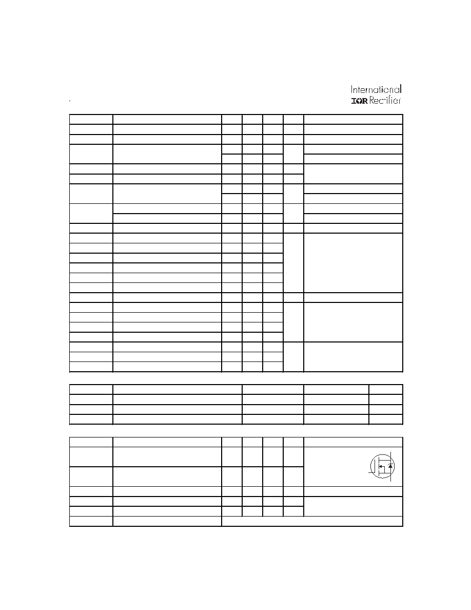
MOSFET symbol
V
GS
= 4.5V, I
D
= 12A
f
V
GS
= 4.5V
Typ.
I
D
= 12A
V
GS
= 0V
V
DS
= 15V
T
J
= 25°C, I
F
= 12A, V
DD
= 15V
di/dt = 100A/µs
f
T
J
= 25°C, I
S
= 12A, V
GS
= 0V
f
showing the
integral reverse
p-n junction diode.
V
DS
= V
GS
, I
D
= 250µA
V
DS
= 24V, V
GS
= 0V
V
DS
= 24V, V
GS
= 0V, T
J
= 125°C
Clamped Inductive Load
V
DS
= 15V, I
D
= 12A
Conditions
V
GS
= 0V, I
D
= 250µA
Reference to 25°C, I
D
= 1mA
V
GS
= 10V, I
D
= 15A
f
Conditions
7.5
Max.
230
12
= 1.0MHz
V
DS
= 16V, V
GS
= 0V
V
DD
= 15V, V
GS
= 4.5V
f
I
D
= 12A
V
DS
= 16V
V
GS
= 20V
V
GS
= -20V
IRLR/U7821
www.irf.com
3
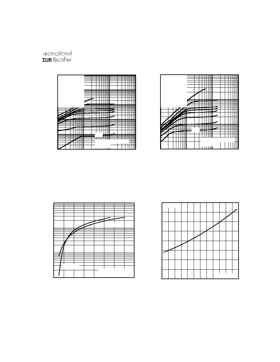
Fig 4. Normalized On-Resistance
vs. Temperature
Fig 2. Typical Output Characteristics
Fig 1. Typical Output Characteristics
Fig 3. Typical Transfer Characteristics
1
10
100
1000
2.0
4.0
6.0
8.0
10.0
V = 15V
20µs PULSE WIDTH
DS
V , Gate-to-Source Voltage (V)
I , D
r
a
i
n
-
to
-
S
o
u
r
c
e
C
u
r
r
e
n
t
(
A
)
GS
D
T = 175 C
J
°
T = 25 C
J
°
-60
-40
-20
0
20
40
60
80
100
120
140
160
180
0.0
0.5
1.0
1.5
2.0
R
, D
r
a
i
n
-
to
-
S
o
u
r
ce
O
n
R
e
si
sta
n
c
e
(
N
or
m
a
l
i
z
ed)
DS
(
o
n
)
°
V
=
I
=
GS
D
10V
65A
0.1
1
10
100
VDS, Drain-to-Source Voltage (V)
0.1
1
10
100
1000
10000
I D
,
D
r
a
i
n
-
t
o
-
S
o
u
r
c
e
C
u
r
r
e
n
t
(
A
)
2.5V
20µs PULSE WIDTH
Tj = 25°C
VGS
TOP
10V
4.5V
3.7V
3.5V
3.3V
3.0V
2.7V
BOTTOM
2.5V
0.1
1
10
100
VDS, Drain-to-Source Voltage (V)
1
10
100
1000
I D
,
D
r
a
i
n
-
t
o
-
S
o
u
r
c
e
C
u
r
r
e
n
t
(
A
)
2.5V
20µs PULSE WIDTH
Tj = 175°C
VGS
TOP
10V
4.5V
3.7V
3.5V
3.3V
3.0V
2.7V
BOTTOM
2.5V
T
J
, Junction Temperature (°C)
IRLR/U7821
4
www.irf.com
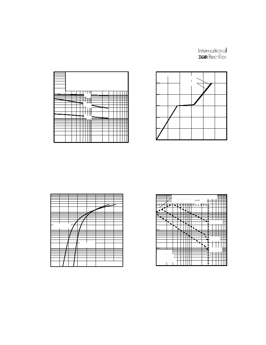
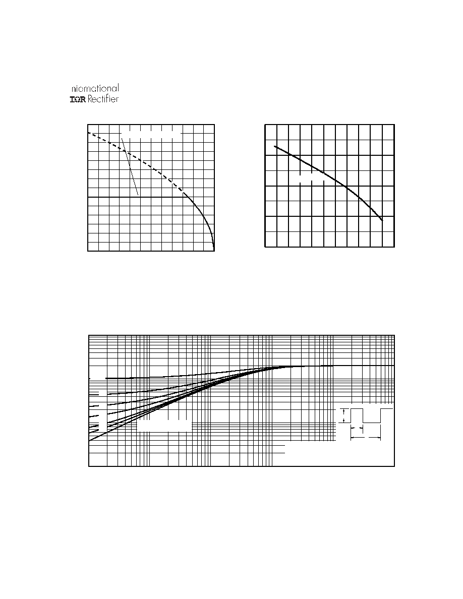
Fig 8. Maximum Safe Operating Area
Fig 6. Typical Gate Charge vs.
Gate-to-Source Voltage
Fig 5. Typical Capacitance Vs.
Drain-to-Source Voltage
Fig 7. Typical Source-Drain Diode
Forward Voltage
1
10
100
VDS, Drain-to-Source Voltage (V)
10
100
1000
10000
C
,
C
a
p
a
c
i
t
a
n
c
e
(
p
F
)
VGS = 0V, f = 1 MHZ
Ciss = Cgs + Cgd, Cds SHORTED
Crss = Cgd
Coss = Cds + Cgd
Coss
Crss
Ciss
0.1
1
10
100
1000
0.0
0.5
1.0
1.5
2.0
V ,Source-to-Drain Voltage (V)
I
,
R
e
v
e
rs
e D
r
ai
n C
u
rrent
(A)
SD
SD
V = 0 V
GS
T = 175 C
J
°
T = 25 C
J
°
1
10
100
VDS, Drain-to-Source Voltage (V)
0.1
1
10
100
1000
I D
,
D
r
a
i
n
-
t
o
-
S
o
u
r
c
e
C
u
r
r
e
n
t
(
A
)
Tc = 25°C
Tj = 175°C
Single Pulse
1msec
10msec
OPERATION IN THIS AREA
LIMITED BY R DS(on)
100µsec
0
2
4
6
8
10
12
QG Total Gate Charge (nC)
0
1
2
3
4
5
6
V
G
S
,
G
a
t
e
-
t
o
-
S
o
u
r
c
e
V
o
l
t
a
g
e
(
V
)
VDS= 24V
VDS= 16V
ID= 12A
IRLR/U7821
www.irf.com
5
Fig 11. Maximum Effective Transient Thermal Impedance, Junction-to-Case
Fig 9. Maximum Drain Current vs.
Case Temperature
25
50
75
100
125
150
175
0
10
20
30
40
50
60
70
T , Case Temperature ( C)
I
,
D
r
ai
n C
u
r
r
ent
(
A
)
°
C
D
LIMITED BY PACKAGE
0.01
0.1
1
10
0.00001
0.0001
0.001
0.01
0.1
1
Notes:
1. Duty factor D =
t / t
2. Peak T
= P
x Z
+ T
1
2
J
DM
thJC
C
P
t
t
DM
1
2
t , Rectangular Pulse Duration (sec)
T
her
m
a
l Res
pons
e
(
Z
)
1
th
JC
0.01
0.02
0.05
0.10
0.20
D = 0.50
SINGLE PULSE
(THERMAL RESPONSE)
-75 -50 -25
0
25
50
75 100 125 150 175 200
TJ , Temperature ( °C )
0.5
1.0
1.5
2.0
2.5
V
G
S
(
t
h
)
G
a
t
e
t
h
r
e
s
h
o
l
d
V
o
l
t
a
g
e
(
V
)
ID = 250µA
Fig 10. Threshold Voltage vs. Temperature