 | ÐлекÑÑоннÑй компоненÑ: IRLR8503 | СкаÑаÑÑ:  PDF PDF  ZIP ZIP |
Äîêóìåíòàöèÿ è îïèñàíèÿ www.docs.chipfind.ru
www.irf.com
1
IRLR8503
Parameter
Symbol IRLR8503
Units
Drain-Source Voltage
V
DS
30
V
Gate-Source Voltage
V
GS
±20
Continuous Drain or Source
T
C
= 25°C
I
D
44
A
T
C
= 90°C
32
Pulsed Drain Current
Q
I
DM
196
Power Dissipation
U
T
C
= 25°C
P
D
62
W
T
C
= 90°C
30
Junction & Storage Temperature Range
T
J
,
T
STG
55 to 150
°C
Continuous Source Current (Body Diode)
I
S
15
A
Pulsed source Current
Q
I
SM
196
· N-Channel Application-Specific MOSFET
· Ideal for CPU Core DC-DC Converters
· Low Conduction Losses
· Minimizes Parallel MOSFETs for high current
applications
Description
This new device employs advanced HEXFET Power
MOSFET technology to achieve very low on-resistance.
The reduced conduction losses makes it ideal for high
efficiency DC-DC converters that power the latest
generation of microprocessors.
The IRLR8503 has been optimized and is 100% tested for
all parameters that are critical in synchronous buck
converters including R
DS(on)
, gate charge and Cdv/dt-
induced turn-on immunity. The IRLR8503 offers an
extremely low combination of Q
sw
& R
DS(on)
for reduced
losses in control FET applications.
The package is designed for vapor phase, infra-red,
convection, or wave soldering techniques. Power
dissipation of greater than 2W is possible in a typical PCB
mount application.
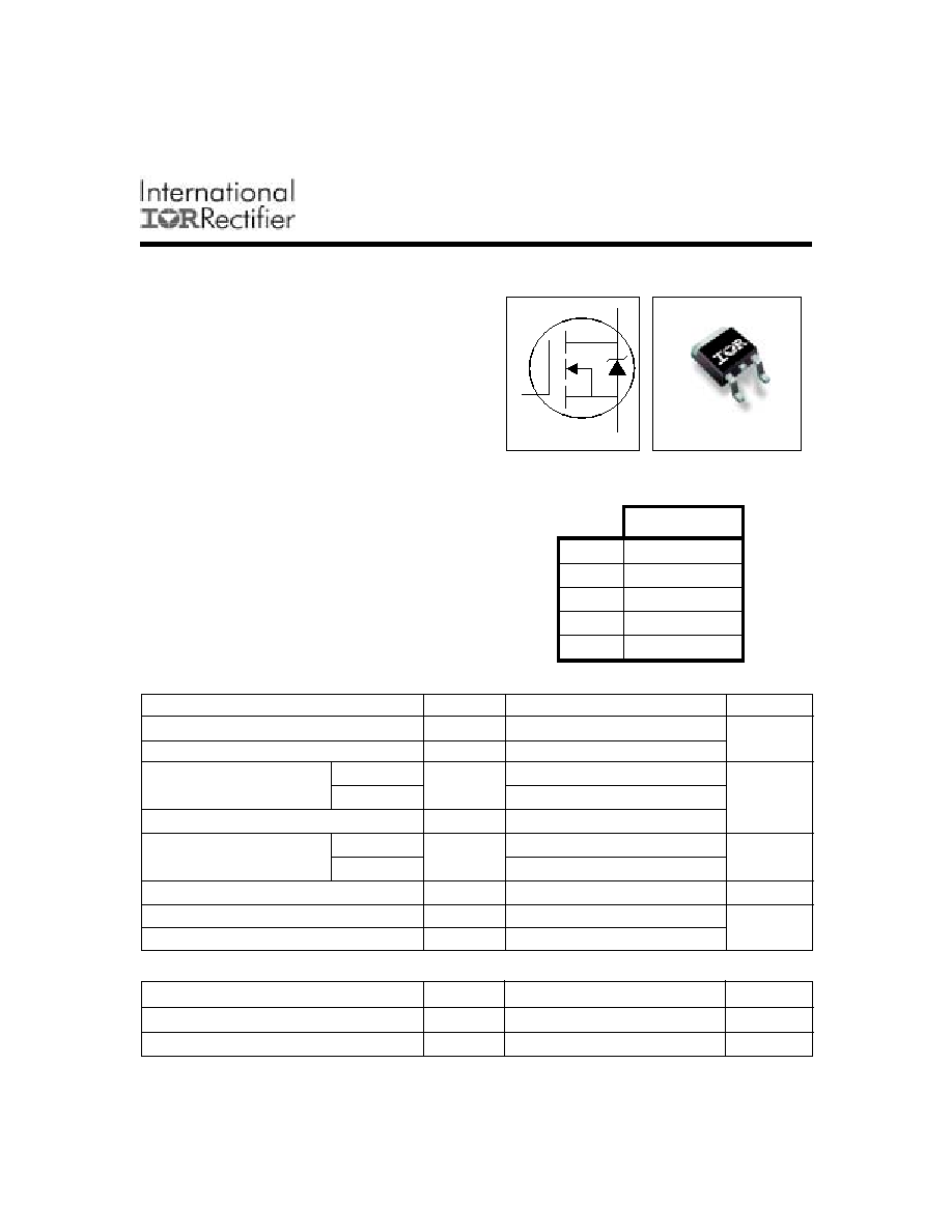
HEXFET
®
MOSFET for DC-DC Converters
IRLR8503
V
DS
30V
R
DS
(on)
18 m
Q
G
20 nC
Q
sw
8 nC
Q
oss
29.5 nC
DEVICE RATINGS (MAX. Values)
IRLR8503
D-Pak
Absolute Maximum Ratings
Parameter
Symbol
Max.
Units
Maximum Junction-to-Ambient
S
R
JA
50
°C/W
Maximum Junction-to-Lead
R
JL
2.0
°C/W
Thermal Resistance
Current (V
GS
10V)
U
S
D
G
PD-93839A
12/21/00
www.irf.com
2
IRLR8503
Parameter
Symbol
Min
Typ
Max
Units
Conditions
Diode Forward Voltage*
V
SD
1.0
V
I
S
= 15A
R
, V
GS
= 0V
Reverse Recovery Charge
T
Q
rr
76
nC
di/dt = 700A/µs
V
DS
= 16V, V
GS
= 0V, I
S
= 15A
Reverse Recovery Charge
Q
rr(s)
67
di/dt = 700A/µs
(with Parallel Schottky)
T
(with 10BQ040)
V
DS
= 16V, V
GS
= 0V, I
S
= 15A
Parameter
Symbol
Min
Typ
Max
Units
Conditions
Drain-to-Source
V
(BR)DSS
30
V
V
GS
= 0V, I
D
= 250µA
Breakdown Voltage*
Static Drain-Source
R
DS
(on)
11
16
m
V
GS
= 10V, I
D
=15A
R
on Resistance*
13 18
V
GS
= 4.5V, I
D
=15A
Gate Threshold Voltage*
V
GS
(th)
1.0
V
V
DS
= V
GS
, I
D
= 250µA
Drain-Source Leakage Current
I
DSS
30*
µA
V
DS
= 24V, V
GS
= 0
150
V
DS
= 24V, V
GS
= 0,
Tj = 100°C
Gate-Source Leakage Current*
I
GSS
±100
nA
V
GS
= ±12V
Total Gate Charge Control FET*
Q
g
15
20
V
GS
= 5V, I
D
= 15A, V
DS
=16V,
Total Gate Charge Sync FET*
Q
g
13
17
V
GS
= 5V, V
DS
< 100mV
Pre-Vth
Q
gs1
3.7
V
DS
= 16V, I
D
= 15A
Gate-Source Charge
Post-Vth
Q
gs2
1.3
nC
Gate-Source Charge
Gate to Drain Charge
Q
gd
4.1
Switch Charge* (Q
gs2
+ Q
gd
)
Q
SW
5.4
8
Output Charge*
Q
oss
23
29.5
V
DS
= 16V, V
GS
= 0
Gate Resistance
R
g
1.7
Turn-on Delay Time
t
d (on)
10
V
DD
= 16V, I
D
= 15A
Drain Voltage Rise Time
tr
v
18
ns
V
GS
= 5V
Turn-off Delay Time
t
d
(off)
11
Clamped Inductive Load
Drain Voltage Fall Time
tf
v
3
See test diagram Fig 14.
Input Capacitance
C
iss
1650
Output Capacitance
C
oss
650
pF
V
DS
= 25V, V
GS
= 0
Reverse Transfer Capacitance
C
rss
58
Electrical Characteristics
Source-Drain Rating & Characteristics
Notes:
Q
Repetitive rating; pulse width limited by max. junction temperature.
R
Pulse width
300 µs; duty cycle
2%.
S
When mounted on 1 inch square copper board, t < 10 sec.
*
Devices are 100% tested to these parameters.
T
Typ = measured - Q
oss
U
Calculated continuous current based on maximum allowable
Junction temperature; switching and other losses will
decrease RMS current capability; package limitation
current = 20A.
www.irf.com
3
IRLR8503
Device Capacitance
Corresponding Charge Parameter
C
GS
Q
GS
C
GS
+ C
GD
Q
G
C
GD
Q
GD
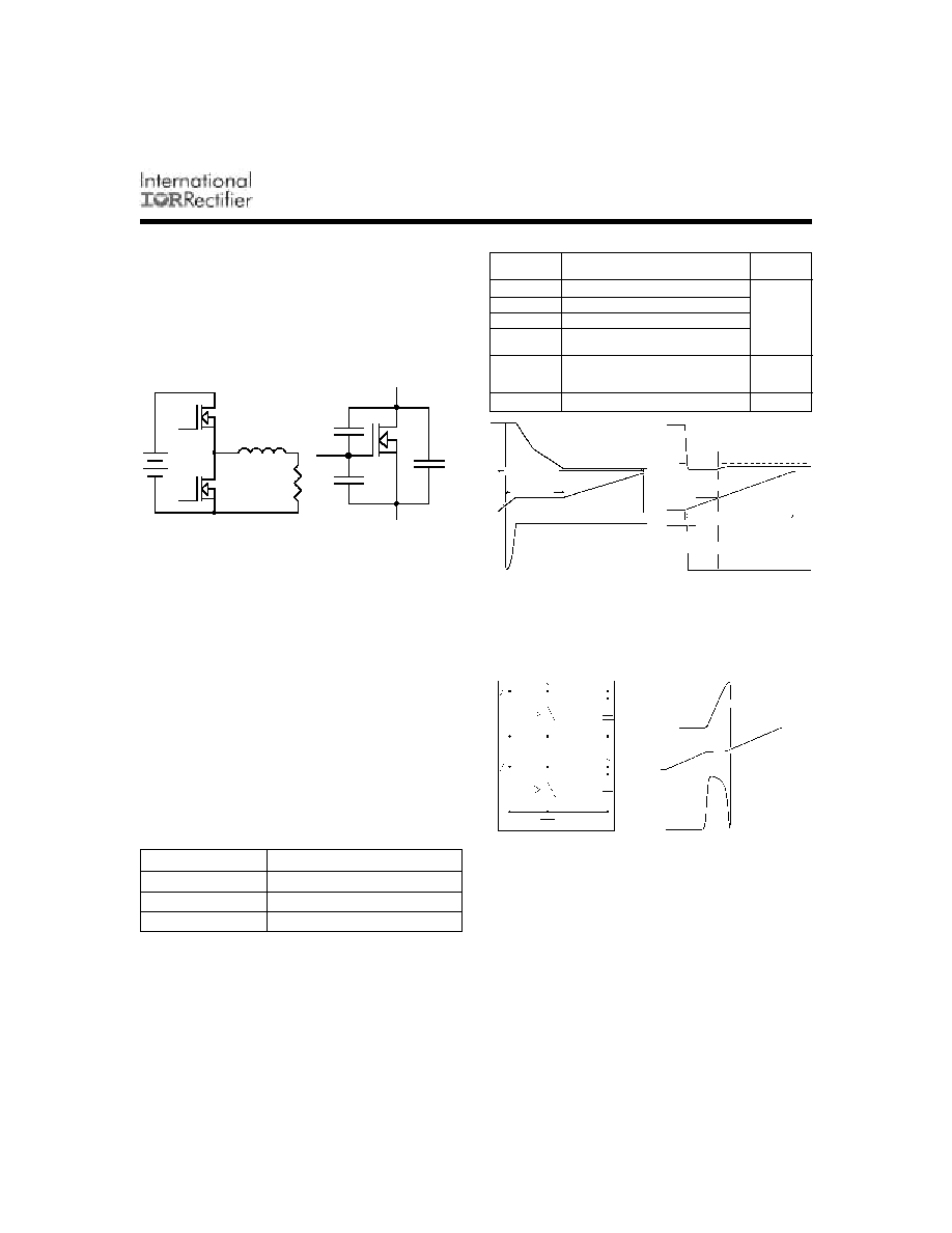
Power MOSFET Optimization for DC-DC Converters
While the IRLR8103V and IRLR8503 can and are be-
ing used in a variety of applications, they were designed
and optimized for low voltage DC-DC conversion in a
synchronous buck converter topology, specifically, mi-
croprocessor power applications. The IRLR8503 (Fig-
ure 1) was optimized for the control FET socket, while
the IRLR8103V was optimized for the synchronous
FET function.
Because of the inter-electrode capacitance (Figure 2)
of the Power MOSFET, specifying the R
DSON
of the de-
vice is not enough to ensure good performance. An
optimization between R
DSON
and charge must be per-
formed to insure the best performing MOSFET for a
given application. Both die size and device architec-
ture must be varied to achieve the minimum possible
in-circuit losses. This is independently true for both
control FET and synchronous FET. Unfortunately, the
capacitances of a FET are non-linear and voltage de-
pendent. Therefore, it is inconvenient to specify and
use them effectively in switching power supply power
loss estimations. This was well understood years ago
and resulted in changing the emphasis from capaci-
tance to gate charge on Power MOSFET data sheets.
International Rectifier has recently taken the industry
a step further by specifying new charge parameters
that are even more specific to DC-DC converter de-
sign (Table 2). In order to understand these parameters,
it is best to start with the in-circuit waveforms in Fig-
ure 3 & Figure 4.
Figure 1 Application
Topology
Figure 2 Inter-electrode
Capacitance
Table 1 Traditional Charge Parameters
Table 2 New Charge Parameters
Figure 3 Control FET
Waveform
Figure 4 Sync FET
Waveform
New Charge
Parameter
Description
Waveform
Q
GS1
Pre-Threshold Gate Charge
Q
GS2
Post-Threshold Gate Charge
Figure 3
Q
GCONT
Control FET Total Q
G
Q
SWITCH
Charge during control FET switching
Combines Q
GS2
and Q
GD
Q
OSS
Output charge
Figure 5
Charge supplied to C
OSS
during the Q
GD
Figure 6
period of control FET switching
Q
GSYNC
Synchronous FET Total Q
G
(V
DS
0)
Figure 4
The waveforms are broken into segments correspond-
ing to charge parameters. These, in turn, correspond
to discrete time segments of the switching waveform.
Losses may be broken into four categories: conduc-
tion loss, gate drive loss, switching loss, and output
loss. The following simplified power loss equation is
true for both MOSFETs in a synchronous buck con-
verter:
For the synchronous FET, the P
SWITCH
term becomes
virtually zero and is ignored.
P
LOSS
= P
CONDUCTION
+ P
GATE DRIVE
+ P
SWITCH
+ P
OUTPUT
Figure 5 Q
OSS
Equivalent Circuit
Figure 6 Q
OSS
Waveforms
Coss1
2 n
IRLR8503
(Cont FET)
IRLR8103V
(Sync FET)
CGD
CGS
CDS
Drain Voltage
Gate Voltage
Drain Current
QGD
QGS1
QGS2
VGTH
QSwitch
QG
(Control FET)
Drain Voltage
0 V
Gate Voltage
0 A
Drain Current
Dead
Time
VGTH
Body
Diode
Current
QG (Sync FET)
g1
g2
N1
Cont FET
N2
Sync FET
SN
Coss2
2n
VIN
Switch node voltage
(VSN)
N1 Gate
Voltage
N1 Current
N1 Coss Discharge
+
N2 Coss Charge
www.irf.com
4
IRLR8503
Table 3 and Table 4 describes the event during the various charge segments and shows an approximation of losses during that
period.
Table 3 Control FET Losses
Table 4 Synchronous FET Losses
Conduction
Loss
Gate Drive
Loss
Switching
Loss
Output
Loss
Losses associated with the Q
OSS
of the device every cycle when the control
FET turns on. Losses are caused by both FETs, but are dissipated by the control
FET.
Segment Losses
Description
Losses associated with MOSFET on time. I
RMS
is a function of load
current and duty cycle.
Losses associated with charging and discharging the gate of the
MOSFET every cycle. Use the control FET Q
G
.
Losses during the drain voltage and drain current transitions for every full cycle.
Losses occur during the Q
GS2
and Q
GD
time period and can be simplified by using
Q
switch
.
)
on
(
DS
RMS
COND
R
I
P
×
=
2
×
×
=
G
G
IN
Q
V
P
×
×
×
×
×
×
×
×
G
SW
L
IN
SWITCH
G
GD
L
IN
QGD
G
GS
L
IN
QGS
I
Q
I
V
P
I
Q
I
V
P
I
Q
I
V
P
2
2
F
V
2
Q
P
IN
OSS
OUTPUT
×
×
=
Conduction
Loss
Gate Drive
Loss
Switching
Loss
Output
Loss
Segment Losses
Description
Losses associated with MOSFET on time. I
RMS
is a function of load current and
duty cycle.
Losses associated with charging and discharging the gate of the MOSFET every
cycle. Use the Sync FET Q
G
.
Generally small enough to ignore except at light loads when the current reverses
in the output inductor. Under these conditions various light load power saving
techniques are employed by the control IC to maintain switching losses to a
negligible level.
Losses associated with the Q
OSS
of the device every cycle when the control FET
turns on. They are caused by the synchronous FET, but are dissipated in the control
FET.
DSon
RMS
COND
R
I
P
×
=
2
×
×
=
G
G
IN
Q
V
P
0
P
SWITCH
×
×
=
IN
OSS
OUTPUT
V
Q
P
2
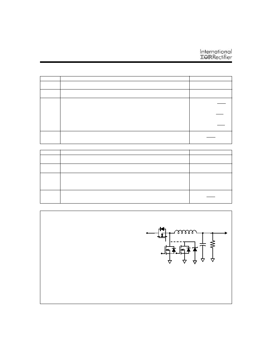
Figure 7. 2 & 3-FET solution for
Synchronous Buck Topology.
IRLR8503
Control FET (Q1)
1 x IRLR8103 or
2 x IRLR8503
Synchronous
FET (Q2)
Typical PC Application
The IRLR8103V and the IRLR8503 are suitable for
Synchronous Buck DC-DC Converters, and are optimized
for use in next generation CPU applications. The
IRLR8103V is primarily optimized for use as the low side
synchronous FET (Q2) with low R
DS(on)
and high CdV/dt
immunity.The IRLR8503 is primarily optimized for use as
the high side control FET (Q2) with low cobmined Qsw and
R
DS(on)
, but can also be used as a synchronous FET. The
IRLR8503 is also tested for Cdv/dt immunity, critical for
the low side socket. The typical configuration in which
these devices may be used in shown in Figure 7.
V
or
www.irf.com
5
IRLR8503
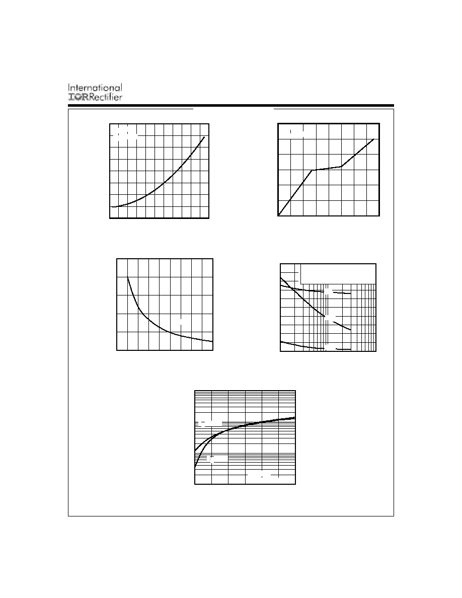
Figure 10. Typical Rds(on) vs. Gate-to-Source Voltage
Figure 8. Normalized On-Resistance vs. Temperature
IRLR8503
Typical Characteristics
Figure 9. Gate-to-Source Voltage vs. Typical Gate
Charge
Figure 11. Typical Capacitance vs. Drain-to-Source Voltage
Figure 12. Typical Transfer Characteristics
100
-60 -40 -20
0
20
40
60
80 100 120 140 160
TJ , Junction Temperature ( °C )
0.5
1.0
1.5
2.0
2.5
R
DS(on)
, Drain-to-Source On Resistance
(Normalized)
ID = 15A
VGS = 4.5V
0
4
8
12
16
QG, Total Gate Charge (nC)
0.0
2.0
4.0
6.0
V
G
S
, Gate-to-Source Voltage (V)
ID= 15A
VDS = 20V
3.0
4.0
5.0
6.0
7.0
8.0
9.0
10.0 11.0 12.0
VGS, Gate -to -Source Voltage (V)
0.010
0.011
0.012
0.013
0.014
0.015
R
DS(on)
, Drain-to -Source O
n Resistance (
)
ID = 15A
1
10
100
0
500
1000
1500
2000
2500
V , Drain-to-Source Voltage (V)
C, Capacitance (pF)
DS
V
C
C
C
=
=
=
=
0V,
C
C
C
f = 1MHz
+ C
+ C
C SHORTED
GS
iss
gs
gd ,
ds
rss
gd
oss
ds
gd
C
iss
C
oss
C
rss
2.5
3.0
3.5
4.0
4.5
5.0
5.5
VGS, Gate-to-Source Voltage (V)
1.0
10.0
100.0
1000.0
I D
, Drain-to-Source Current
(
)
TJ = 25°C
TJ = 150°C
VDS = 15V
20µs PULSE WIDTH