 | ÐлекÑÑоннÑй компоненÑ: IRLU2705 | СкаÑаÑÑ:  PDF PDF  ZIP ZIP |
Äîêóìåíòàöèÿ è îïèñàíèÿ www.docs.chipfind.ru
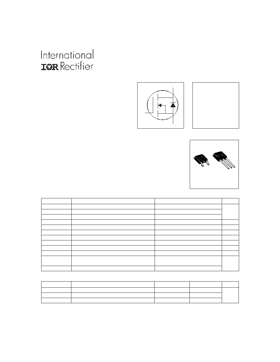
IRLR/U2705
HEXFET
®
Power MOSFET
S
D
G
Parameter
Typ.
Max.
Units
R
JC
Junction-to-Case
2.2
R
JA
Case-to-Ambient (PCB mount)**
50
°C/W
R
JA
Junction-to-Ambient
110
Thermal Resistance
V
DSS
= 55V
R
DS(on)
= 0.040
I
D
= 28A
Description
4/1/03
www.irf.com
1
D-Pak
TO-252AA
I-Pak
TO-251AA
l
Logic-Level Gate Drive
l
Ultra Low On-Resistance
l
Surface Mount (IRLR2705)
l
Straight Lead (IRLU2705)
l
Advanced Process Technology
l
Fast Switching
l
Fully Avalanche Rated
Fifth Generation HEXFETs from International Rectifier utilize advanced
processing techniques to achieve the lowest possible on-resistance per
silicon area. This benefit, combined with the fast switching speed and
ruggedized device design that HEXFET Power MOSFETs are well known for,
provides the designer with an extremely efficient device for use in a wide
variety of applications.
The D-PAK is designed for surface mounting using vapor phase, infrared, or
wave soldering techniques. The straight lead version (IRFU series) is for
through-hole mounting applications. Power dissipation levels up to 1.5 watts
are possible in typical surface mount applications.
** When mounted on 1" square PCB (FR-4 or G-10 Material ) .
For recommended footprint and soldering techniques refer to application note #AN-994
Parameter
Max.
Units
I
D
@ T
C
= 25°C
Continuous Drain Current, V
GS
@ 10V
28
I
D
@ T
C
= 100°C
Continuous Drain Current, V
GS
@ 10V
20
A
I
DM
Pulsed Drain Current
110
P
D
@T
C
= 25°C
Power Dissipation
68
W
Linear Derating Factor
0.45
W/°C
V
GS
Gate-to-Source Voltage
± 16
V
E
AS
Single Pulse Avalanche Energy
110
mJ
I
AR
Avalanche Current
16
A
E
AR
Repetitive Avalanche Energy
6.8
mJ
dv/dt
Peak Diode Recovery dv/dt
5.0
V/ns
T
J
Operating Junction and
-55 to + 175
T
STG
Storage Temperature Range
Soldering Temperature, for 10 seconds
300 (1.6mm from case )
°C
Absolute Maximum Ratings
PD- 91317C
IRLR/U2705
2
www.irf.com
S
D
G
Parameter
Min. Typ. Max. Units
Conditions
I
S
Continuous Source Current
MOSFET symbol
(Body Diode)
showing the
I
SM
Pulsed Source Current
integral reverse
(Body Diode)
p-n junction diode.
V
SD
Diode Forward Voltage
1.3
V
T
J
= 25°C, I
S
= 17A, V
GS
= 0V
t
rr
Reverse Recovery Time
76
110
ns
T
J
= 25°C, I
F
= 16A
Q
rr
Reverse RecoveryCharge
190
290
nC
di/dt = 100A/µs
t
on
Forward Turn-On Time
Intrinsic turn-on time is negligible (turn-on is dominated by L
S
+L
D
)
Source-Drain Ratings and Characteristics
28
110
A
V
DD
= 25V, starting T
J
= 25°C, L = 610µH
R
G
= 25
, I
AS
= 16A. (See Figure 12)
Repetitive rating; pulse width limited by
max. junction temperature. ( See fig. 11 )
Pulse width
300µs; duty cycle
2%.
This is applied for I-PAK, L
S
of D-PAK is measured between
lead and center of die contact.
Uses IRLZ34N data and test conditions.
I
SD
16A, di/dt
270A/µs, V
DD
V
(BR)DSS
,
T
J
175°C
Notes:
Parameter
Min. Typ. Max. Units
Conditions
V
(BR)DSS
Drain-to-Source Breakdown Voltage
55
V
V
GS
= 0V, I
D
= 250µA
V
(BR)DSS
/
T
J
Breakdown Voltage Temp. Coefficient
0.065
V/°C
Reference to 25°C, I
D
= 1mA
0.040
V
GS
= 10V, I
D
= 17A
0.051
W
V
GS
= 5.0V, I
D
= 17A
0.065
V
GS
= 4.0V, I
D
= 14A
V
GS(th)
Gate Threshold Voltage
1.0
2.0
V
V
DS
= V
GS
, I
D
= 250µA
g
fs
Forward Transconductance
11
S
V
DS
= 25V, I
D
= 16A
25
µA
V
DS
= 55V, V
GS
= 0V
250
V
DS
= 44V, V
GS
= 0V, T
J
= 150°C
Gate-to-Source Forward Leakage
100
nA
V
GS
= 16V
Gate-to-Source Reverse Leakage
-100
V
GS
= -16V
Q
g
Total Gate Charge
25
I
D
= 16A
Q
gs
Gate-to-Source Charge
5.2
nC
V
DS
= 44V
Q
gd
Gate-to-Drain ("Miller") Charge
14
V
GS
= 5.0V, See Fig. 6 and 13
t
d(on)
Turn-On Delay Time
8.9
V
DD
= 28V
t
r
Rise Time
100
ns
I
D
= 16A
t
d(off)
Turn-Off Delay Time
21
R
G
= 6.5
,
V
GS
= 5.0V
t
f
Fall Time
29
R
D
= 1.8
,
See Fig. 10
Between lead,
6mm (0.25in.)
from package
and center of die contact
C
iss
Input Capacitance
880
V
GS
= 0V
C
oss
Output Capacitance
220
pF
V
DS
= 25V
C
rss
Reverse Transfer Capacitance
94
= 1.0MHz, See Fig. 5
Electrical Characteristics @ T
J
= 25°C (unless otherwise specified)
nH
I
GSS
S
D
G
L
S
Internal Source Inductance
7.5
R
DS(on)
Static Drain-to-Source On-Resistance
L
D
Internal Drain Inductance
4.5
I
DSS
Drain-to-Source Leakage Current
Caculated continuous current based on maximum allowable
junction temperature; Package limitation current = 20A.
IRLR/U2705
www.irf.com
3
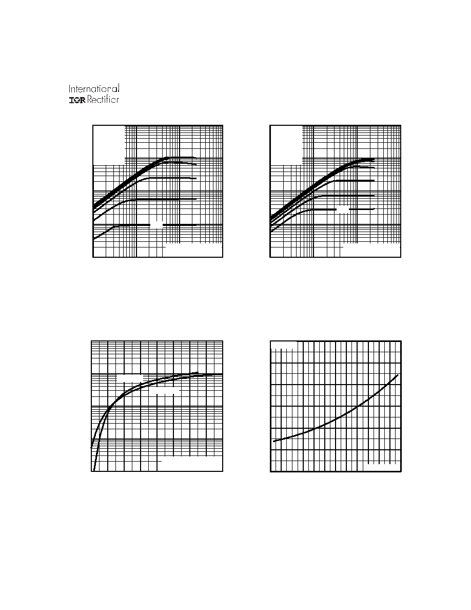
Fig 4. Normalized On-Resistance
Vs. Temperature
Fig 2. Typical Output Characteristics
Fig 1. Typical Output Characteristics
Fig 3. Typical Transfer Characteristics
0.1
1
10
100
1000
0.1
1
10
100
I
, D
r
a
i
n
-
to-S
ou
rce Curre
nt (A
)
D
V , Drain-to-Source Voltage (V)
DS
A
20µs PULSE WIDTH
T = 175°C
VGS
TOP 15V
12V
10V
8.0V
6.0V
4.0V
3.0V
BOTTOM 2.5V
2.5V
J
0.1
1
10
100
1000
0.1
1
10
100
I
, D
r
a
i
n
-
to
-So
u
rc
e
Cu
rre
n
t
(A
)
D
V , Drain-to-Source Voltage (V)
DS
A
20µs PULSE WIDTH
T = 25°C
J
VGS
TOP 15V
12V
10V
8.0V
6.0V
4.0V
3.0V
BOTTOM 2.5V
2.5V
0.1
1
10
100
1000
2
3
4
5
6
7
8
9
10
T = 25°C
J
GS
V , Gate-to-Source Voltage (V)
D
I
,
Drain-t
o
-
S
ou
rce C
u
rr
e
n
t
(
A
)
T = 175°C
J
A
V = 25V
20µs PULSE WIDTH
DS
0.0
0.5
1.0
1.5
2.0
2.5
3.0
-60 -40 -20
0
20
40
60
80
100 120 140 160 180
J
T , Junction Temperature (°C)
R
, Dra
i
n
-
to
-
S
o
u
r
c
e
On
Re
s
i
s
t
a
n
c
e
DS
(o
n)
(N
orm
a
l
i
zed
)
V = 10V
GS
A
I = 27A
D
IRLR/U2705
4
www.irf.com
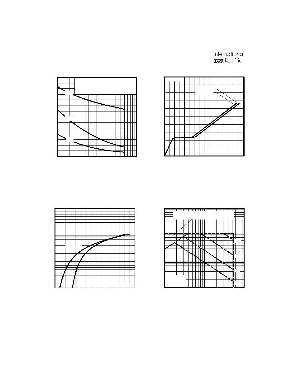
Fig 8. Maximum Safe Operating Area
Fig 6. Typical Gate Charge Vs.
Gate-to-Source Voltage
Fig 5. Typical Capacitance Vs.
Drain-to-Source Voltage
Fig 7. Typical Source-Drain Diode
Forward Voltage
0
200
400
600
800
1000
1200
1400
1
10
100
C,
Capac
i
t
a
n
c
e
(
p
F)
DS
V , Drain-to-Source Voltage (V)
A
V = 0V, f = 1MHz
C = C + C , C SHORTED
C = C
C = C + C
GS
iss gs gd ds
rss gd
oss ds gd
C
iss
C
oss
C
rss
0
3
6
9
12
15
0
4
8
12
16
20
24
28
32
Q , Total Gate Charge (nC)
G
V
, Ga
te
-to
-
S
o
u
r
c
e
V
o
lta
g
e
(
V
)
GS
A
FOR TEST CIRCUIT
SEE FIGURE 13
I = 16A
V = 44V
V = 28V
D
DS
DS
1
10
100
1000
0.4
0.6
0.8
1.0
1.2
1.4
1.6
1.8
2.0
T = 25°C
J
V = 0V
GS
V , Source-to-Drain Voltage (V)
I
,
Rever
s
e Dr
ai
n C
u
r
r
ent
(
A
)
SD
SD
A
T = 175°C
J
1
10
100
1000
1
10
100
V , Drain-to-Source Voltage (V)
DS
I
,
Dr
ai
n Cur
r
e
nt
(
A
)
OPERATION IN THIS AREA LIMITED
BY R
D
DS(on)
10µs
100µs
1ms
10ms
A
T = 25°C
T = 175°C
Single Pulse
C
J
IRLR/U2705
www.irf.com
5
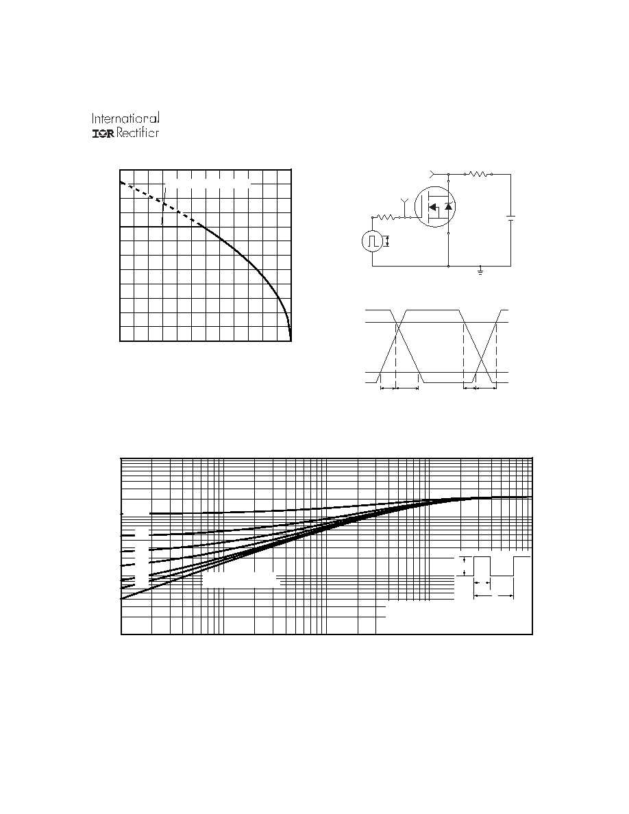
Fig 10a. Switching Time Test Circuit
V
DS
90%
10%
V
GS
t
d(on)
t
r
t
d(off)
t
f
Fig 10b. Switching Time Waveforms
V
DS
Pulse Width 1 µs
Duty Factor 0.1 %
R
D
V
GS
R
G
D.U.T.
5V
+
-
V
DD
Fig 11. Maximum Effective Transient Thermal Impedance, Junction-to-Case
Fig 9. Maximum Drain Current Vs.
Case Temperature
0.01
0.1
1
10
0.00001
0.0001
0.001
0.01
0.1
Notes:
1. Duty factor D = t / t
2. Peak T = P
x Z
+ T
1
2
J
DM
thJC
C
P
t
t
DM
1
2
t , Rectangular Pulse Duration (sec)
Thermal Res
pons
e
(
Z
)
1
thJC
0.01
0.02
0.05
0.10
0.20
D = 0.50
SINGLE PULSE
(THERMAL RESPONSE)
25
50
75
100
125
150
175
0
5
10
15
20
25
30
T , Case Temperature ( C)
I , Drain Current (A)
°
C
D
LIMITED BY PACKAGE