IRU1205
IRU1205-18 / IRU1205-25 / IRU1205-28
IRU1205-30 / IRU1205-33 / IRU1205-36
1
Rev. 2.3
07/16/02
www.irf.com
DESCRIPTION
The IRU1205 device is an efficient linear voltage regula-
tor with better than 1% initial voltage accuracy, very low
dropout voltage and very low ground current designed
especially for hand held, battery powered applications.
Other features of the device are: TTL compatible enable/
shutdown control input, current limiting and thermal shut-
down.
The IRU1205 is available in fixed and adjustable output
voltage versions in a small SOT-23 5-Pin package.
300mA ULTRA LOW DROPOUT POSITIVE
ADJUSTABLE AND FIXED REGULATORS
SOT-23 Package
Stable with 2.2
m
F Ceramic Capacitor
1% Voltage Reference Accuracy
Only 270mV Dropout at 300mA
and 170mV Dropout at 150mA
5
m
A Quiescent Current in Shutdown
Current Limit and Thermal Shutdown
Logic Input Enable Pin
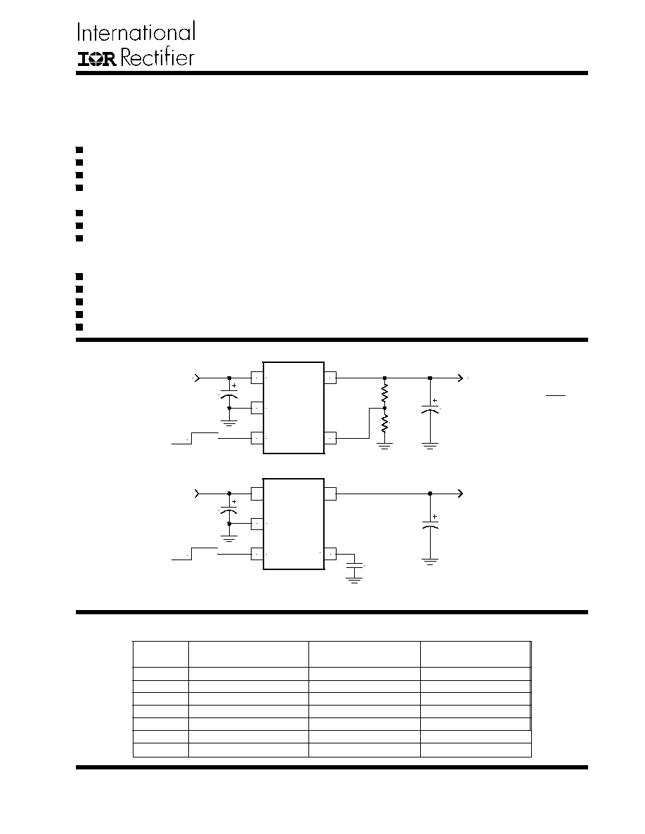
TYPICAL APPLICATION
Figure 1 - Typical application of the IRU1205 ajustable voltage regulator.
Figure 2 - Typical application of the IRU1205-25 fixed voltage regulator.
Data Sheet No. PD94133
APPLICATIONS
Laptop, Notebook & Palmtop computers
Battery Powered Equipments
PCMCIA Vcc & Vpp Regulator
Consumer Electronics
High Efficiency Linear Power Supplies
FEATURES
PACKAGE ORDER INFORMATION
T
J
(
�C) 5-PIN SOT-23 OUTPUT
SOT-23 (L5) MARKING VOLTAGE
0 To 125 IRU1205CL AT00 Adj
0 To 125 IRU1205-18CL AT18 1.8V
0 To 125 IRU1205-25CL AT25 2.5V
0 To 125 IRU1205-28CL AT28 2.8V
0 To 125 IRU1205-30CL AT30 3.0V
0 To 125 IRU1205-33CL AT33 3.3V
0 To 125 IRU1205-36CL AT36 3.6V
V
IN
V
OUT
R1
R2
C1
2.2uF
C2
2.2uF
SD Enable
5
3
4
V
OUT
Adj
2
1
V
IN
Gnd
En
3.3V
2.5V
C3
1000pF
C1
2.2uF
C2
2.2uF
SD
Enable
5
3
4
V
OUT
C
BYP
2
1
V
IN
Gnd
En
Vo = 1.25
3
1+ R1
R2
(
)

2
Rev. 2.3
07/16/02
IRU1205
IRU1205-18 / IRU1205-25 / IRU1205-28
IRU1205-30 / IRU1205-33 / IRU1205-36
www.irf.com
ABSOLUTE MAXIMUM RATINGS
Input Voltage (V
IN
) ..................................................... 10V
Enable Input Voltage ................................................. 10V
Storage Temperature Range ....................................... -65�C To 150�C
Operating Junction Temperature Range ...................... 0�C To 150�C
PACKAGE INFORMATION
5-PIN SOT-23 (L5) 5-PIN SOT-23 (L5)
ELECTRICAL SPECIFICATIONS
Reference Voltage
(See Table 1 for typical values)
Line Regulation
Load Regulation (Note 1)
Dropout Voltage (Note 2)
Ground Current (Note 3)
Ground Current-SD Activated
Current Limit
Thermal Regulation
Adjust Pin Current
Enable Pin Input LO Voltage
Enable Pin Input HI Voltage
Enable Pin Input LO Current
Enable Pin Input HI Current
u
JA
=256
8
C/W
u
JA
=256
8
C/W
Unless otherwise specified, these specifications apply over C
IN
=Co=22
m
F, Io=100
m
A, V
IN(MIN)
=2.5V(Adjustable
devices) V
IN
=Vo + 1V(for fixed voltage devices), V
OUT
=V
FB
(for adjustable version only), C
BYP
=470pF(for AT18, AT25,
AT28, AT30, AT33 and AT36), V
ENB
=2V and T
A
=25
8
C. Typical values refer to T
A
=25
8
C. Low duty cycle pulse testing
is used which keeps junction and case temperatures equal to the ambient temperature.
En
Adj
Gnd V
IN
V
OUT
AT00
Adjustable
3
2
1
4
5
Fixed
En
C
BYP
Gnd V
IN
V
OUT
ATxx
3
2
1
4
5
PARAMETER
SYM TEST CONDITION
MIN TYP MAX UNITS
(Note 4)
Vo + 1V<V
IN
<10V
1mA<Io<100mA
100mA<Io<300mA
Io=100
m
A
Io=100
m
A (Note 4)
Io=50mA
Io=50mA (Note 4)
Io=150mA
Io=150mA (Note 4)
Io=300mA
Io=300mA (Note 4)
V
EN
=2V, Io=100
m
A
Io=100
m
A (Note 4)
Io=50mA
Io=50mA (Note 4)
Io=150mA
Io=150mA (Note 4)
Io=300mA
Io=300mA (Note 4)
V
EN
=0V to 0.8V or Open
Vo=0V
V
IN
=10V, Io=150mA, 10ms Pulse
V
IN
=2.5V, Vo=V
ADJ
Regulator OFF
Regulator ON
V
EN(L)
=0V to 0.8V
V
EN(H)
=2V to V
IN
-1
-2
320
2
0.005
0.8
0.1
10
13
85
100
170
204
270
324
120
240
420
540
2200
2900
7200
9300
5
420
0.05
0.1
0.01
20
1
2
50
70
110
140
220
260
350
400
160
600
2900
9500
0.8
%
%/V
%
mV
m
A
m
A
mA
%/W
m
A
V
V
m
A
m
A
Vo
D
V
I
D
V
L
D
V
I(O)
I
Q
I
Q(SD)
I
CL
D
V
P
I
ADJ
V
EN(L)
V
EN(H)
IRU1205
IRU1205-18 / IRU1205-25 / IRU1205-28
IRU1205-30 / IRU1205-33 / IRU1205-36
3
Rev. 2.3
07/16/02
www.irf.com
PIN # PIN SYMBOL PIN DESCRIPTION
The input pin of the regulator. Typically a large storage capacitor is connected from
this pin to ground to insure that the input voltage does not sag below the minimum
drop out voltage during the load transient response. This pin must always be higher
than V
OUT
by at least the amount of the dropout voltage and some margin in order for
the device to regulate properly.
Ground pin. This pin must be connected to the lowest potential in the system and all
other pins must be at higher potential with respect to this pin.
Enable pin. A low signal or left open on this pin shuts down the output. This pin must
be tied HI or to V
IN
for normal operation.
A resistor divider from this pin to the V
OUT
pin and ground sets the output voltage. To
minimize the error due to the error amplifier, select the values of the resistor dividers
to be less than 10K
V
.
A 470 to 1000pF bypass capacitor connected to this pin reduces the output noise.
The output of the regulator. A minimum of 2.2
m
F with max ESR of 1
V
capacitor must
be connected from this pin to ground to insure stability.
5-PIN Output
SOT-23 Voltage
IRU1205 1.25V
IRU1205-18 1.8V
IRU1205-25 2.5V
IRU1205-28 2.8V
IRU1205-30 3.0V
IRU1205-33 3.3V
IRU1205-36 3.6V
Note 3:
Ground current is the regulator quiescent cur-
rent plus the pass transistor current. The total current
from the supply is the sum of the load current plus the
ground pin current.
Note 4:
The specification applies for the junction tem-
perature of 0 to +125
8
C.
Note 1:
Low duty cycle pulse testing with Kelvin con-
nections is required in order to maintain accurate data.
Note 2:
Dropout voltage is defined as the minimum dif-
ferential voltage between V
IN
and V
OUT
required to main-
tain regulation at V
OUT
. It is measured when the output
voltage drops 1% below its nominal value.
PIN DESCRIPTIONS
The output voltage of the adjustable device can be set
using:
Where:
R1 = Resistor connected from output to the Adj pin
R2 = Resistor connected from Adj pin to Gnd
1
2
3
4
4
5
V
IN
Gnd
En
Adj
(Adjustable Only)
C
BYP
(Fixed Only)
V
OUT
Table 1- Nominal output voltage vs. part number.
Vo = 1.25
3
1+ R1
R2
(
)

4
Rev. 2.3
07/16/02
IRU1205
IRU1205-18 / IRU1205-25 / IRU1205-28
IRU1205-30 / IRU1205-33 / IRU1205-36
www.irf.com
BLOCK DIAGRAM
Figure 3 - IRU1205 Adjustable output block diagram.
Figure 4 - IRU1205-18, IRU1205-25, IRU1205-28, IRU1205-30, IRU1205-33 and
IRU1205-36 Fixed output block diagram.
IR WORLD HEADQUARTERS:
233 Kansas St., El Segundo, California 90245, USA Tel: (310) 252-7105
TAC Fax: (310) 252-7903
Visit us at www.irf.com for sales contact information
Data and specifications subject to change without notice. 02/01
V
IN
En
THERMAL
SHUTDOWN
1.25V
V
OUT
Adj
Gnd
+
1
4
2
3
5
V
IN
En
THERMAL
SHUTDOWN
1.25V
V
OUT
C
BYP
Gnd
+
1
4
2
3
5
IRU1205
IRU1205-18 / IRU1205-25 / IRU1205-28
IRU1205-30 / IRU1205-33 / IRU1205-36
5
Rev. 2.3
07/16/02
www.irf.com
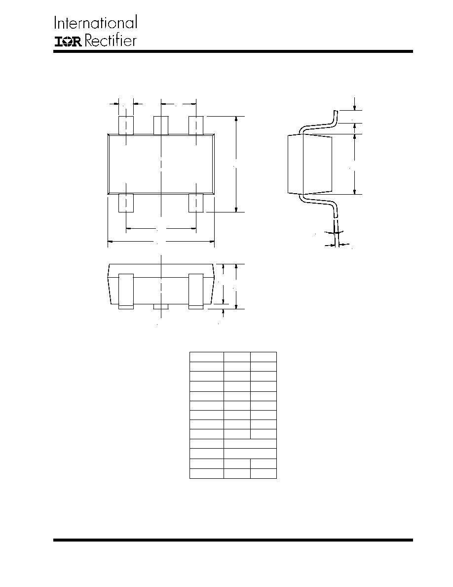
(L5) SOT-23 Package
5-Pin
SYMBOL
A
A1
A2
B
C
D
E
E1
e
e1
L
a
MIN
0.90
0.00
0.90
0.25
0.09
2.80
2.60
1.50
0.35
0
8
MAX
1.45
0.15
1.30
0.50
0.20
3.00
3.00
1.75
0.55
10
8
0.95 REF
1.90 REF
NOTE: ALL MEASUREMENTS
ARE IN MILLIMETERS.
CL
E
C
E1
L
B
e
D
e1
A
A2
A1
a

6
Rev. 2.3
07/16/02
IRU1205
IRU1205-18 / IRU1205-25 / IRU1205-28
IRU1205-30 / IRU1205-33 / IRU1205-36
www.irf.com
PKG
DESIG
L5
PACKAGE
DESCRIPTION
SOT-23
PARTS
PER TUBE
---
PARTS
PER REEL
3000
PACKAGE SHIPMENT METHOD
PIN
COUNT
5
T & R
Orientation
Fig A
Feed Direction
Figure A
1
1
1
IR WORLD HEADQUARTERS:
233 Kansas St., El Segundo, California 90245, USA Tel: (310) 252-7105
TAC Fax: (310) 252-7903
Visit us at www.irf.com for sales contact information
Data and specifications subject to change without notice. 02/01