Äîêóìåíòàöèÿ è îïèñàíèÿ www.docs.chipfind.ru
Product Summary
Part Number
BV
DSS
R
DS(on)
I
D
IRFE430
500V
1.50
2.5A
Features:
n
Hermetically Sealed
n
Simple Drive Requirements
n
Ease of Paralleling
n
Small footprint
n
Surface Mount
n
Lightweight
N-CHANNEL
Provisional Data Sheet No. PD - 9.1719
500Volt, 1.50
, HEXFET
The leadless chip carrier (LCC) package represents
the logical next step in the continual evolution of
surface mount technology. The LCC provides
designers the extra flexibility they need to increase
circuit board density. International Rectifier has
engineered the LCC package to meet the specific
needs of the power market by increasing the size of
the bottom source pad, thereby enhancing the
thermal and electrical performance. The lid of the
package is grounded to the source to reduce RF
interference.
HEXFET transistors also feature all of the well-es-
tablished advantages of MOSFETs, such as volt-
age control, very fast switching, ease of paralleling
and electrical parameter temperature stability. They
are well-suited for applications such as switching
power supplies, motor controls, inverters, choppers,
audio amplifiers and high-energy pulse circuits, and
virtually any application where high reliability is re-
quired.
12/3097
Absolute Maximum Ratings
Parameter
IRFE430, JANTX-, JANTXV-, 2N6802U
Units
ID @ VGS = 10V, TC = 25°C
Continuous Drain Current
2.5
ID @ VGS = 10V, TC = 100°C Continuous Drain Current
1.5
IDM
Pulsed Drain Current
11
PD @ TC = 25°C
Max. Power Dissipation
25
W
Linear Derating Factor
0.20
W/K
VGS
Gate-to-Source Voltage
±20
V
EAS
Single Pulse Avalanche Energy
0.31
mJ
dv/dt
Peak Diode Recovery dv/dt
6.2
V/ns
TJ
Operating Junction
-55 to 150
TSTG
Storage Temperature Range
Surface Temperature
300 ( for 5 seconds)
Weight
0.42 (typical)
g
o
C
A
IRFE430
REPETITIVE AVALANCHE AND dv/dt RATED
JANTX2N6802U
HEXFET
®
TRANSISTOR
JANTXV2N6802U
[REF:MIL-PRF-19500/557]
2
www.irf.com
IRFE430, JANTX-, JANTXV-, 2N6802U Device
Electrical Characteristics
@ Tj = 25°C (Unless Otherwise Specified)
Parameter
Min
Typ Max Units
Test Conditions
BVDSS
Drain-to-Source Breakdown Voltage
500
--
--
V
VGS =0 V, ID = 1.0mA
BVDSS/
TJ Temperature Coefficient of Breakdown
--
0.59
--
V/°C
Reference to 25°C, ID = 1.0mA
Voltage
RDS(on)
Static Drain-to-Source
--
--
1.50
VGS = 10V, ID = 1.5A
On-State Resistance
--
--
1.725
VGS = 10V, ID = 2.5A
VGS(th)
Gate Threshold Voltage
2.0
--
4.0
V
VDS = VGS, ID = 250µA
gfs
Forward Transconductance
2.0
--
--
S (
)
VDS > 15V, IDS = 1.5A
IDSS
Zero Gate Voltage Drain Current
--
--
25
VDS= 0.8 x Max Rating,VGS=0V
--
--
250
VDS = 0.8 x Max Rating
VGS = 0V, TJ = 125°C
IGSS
Gate-to-Source Leakage Forward
--
--
100
VGS = 20 V
IGSS
Gate-to-Source Leakage Reverse
--
--
-100
VGS = -20V
Qg
Total Gate Charge
--
--
30
VGS = 10V, ID = 2.5A
Qgs
Gate-to-Source Charge
--
--
4.5
nC
VDS = Max Rating x 0.5
Qgd
Gate-to-Drain (`Miller') Charge
--
--
28
td
(on)
Turn-On Delay Time
--
--
30
VDD = 250V, ID = 2.5A,
tr
Rise Time
--
--
30
RG = 7.5
td
(off)
Turn-Off Delay Time
--
--
55
tf
Fall Time
--
--
30
LD
Internal Drain Inductance
--
1.8
--
LS
Internal Source Inductance
--
4.3
--
Ciss
Input Capacitance
--
750
--
VGS = 0V, VDS = 25 V
Coss
Output Capacitance
--
240
--
pF
f = 1.0MHz
Crss
Reverse Transfer Capacitance
--
67
--
Source-Drain Diode Ratings and Characteristics
Parameter
Min Typ Max Units
Test Conditions
IS
Continuous Source Current (Body Diode)
--
--
2.5
ISM
Pulse Source Current (Body Diode)
--
--
11
VSD
Diode Forward Voltage
--
--
1.4
V
T
j
= 25°C, IS = 2.5A, VGS = 0V
trr
Reverse Recovery Time
--
--
900
ns
Tj = 25°C, IF = 2.5A, di/dt
100A/
µ
s
QRR
Reverse Recovery Charge
--
--
2.0
µC
VDD
50V
ton
Forward Turn-On Time
Intrinsic turn-on time is negligible. Turn-on speed is substantially controlled by LS + LD.
A
Modified MOSFET symbol
showing the integral reverse
p-n junction rectifier.
nA
nH
ns
Measured from drain pad to
die.
Measured from center of
source pad to the end of
source bonding wire.
Modified MOSFET symbol show-
ing the internal inductances.
µ
A
Thermal Resistance
Parameter
Min Typ Max
Units
Test Conditions
RthJC
Junction-to-Case
--
--
5.0
K/W
RthJPCB
Junction-to-PC Board
--
--
19
Soldered to a copper clad PC board
Details of notes
through
are on the last page
www.irf.com
3
IRFE430, JANTX-, JANTXV-, 2N6802U Device
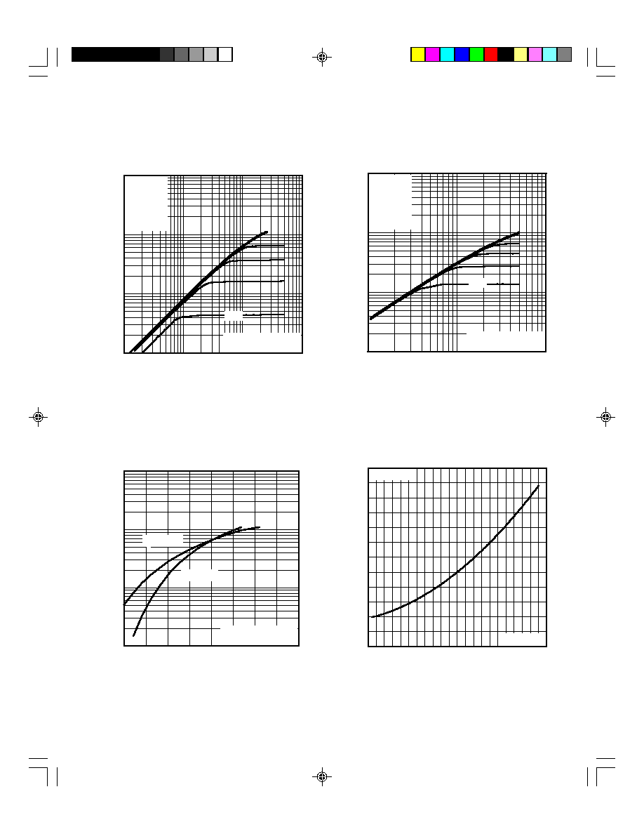
Fig 4. Normalized On-Resistance
Vs. Temperature
Fig 2. Typical Output Characteristics
Fig 1. Typical Output Characteristics
Fig 3. Typical Transfer Characteristics
0.1
1
10
100
0.1
1
10
100
20µs PULSE WIDTH
T = 25 C
J
°
TOP
BOTTOM
VGS
15V
10V
8.0V
7.0V
6.0V
5.5V
5.0V
4.5V
V , Drain-to-Source Voltage (V)
I , Drain-to-Source Current (A)
DS
D
4.5V
0.1
1
10
100
1
10
100
20µs PULSE WIDTH
T = 150 C
J
°
TOP
BOTTOM
VGS
15V
10V
8.0V
7.0V
6.0V
5.5V
5.0V
4.5V
V , Drain-to-Source Voltage (V)
I , Drain-to-Source Current (A)
DS
D
4.5V
-60 -40 -20
0
20
40
60
80 100 120 140 160
0.0
0.5
1.0
1.5
2.0
2.5
3.0
T , Junction Temperature ( C)
R , Drain-to-Source On Resistance
(Normalized)
J
DS(on)
°
V
=
I =
GS
D
10V
2.5A
0.1
1
10
100
4.0
5.0
6.0
7.0
8.0
V = 50V
20µs PULSE WIDTH
DS
V , Gate-to-Source Voltage (V)
I , Drain-to-Source Current (A)
GS
D
T = 25 C
J
°
T = 150 C
J
°
4
www.irf.com
IRFE430, JANTX-, JANTXV-, 2N6802U Device
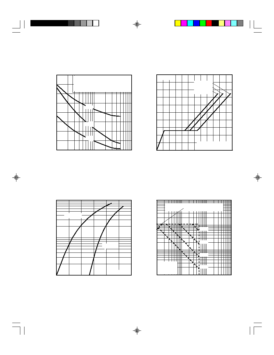
Fig 8. Maximum Safe Operating Area
Fig 6. Typical Gate Charge Vs.
Gate-to-Source Voltage
Fig 7. Typical Source-Drain Diode
Forward Voltage
0.1
1
10
0.4
0.6
0.8
1.0
V ,Source-to-Drain Voltage (V)
I , Reverse Drain Current (A)
SD
SD
V = 0 V
GS
T = 25 C
J
°
T = 150 C
J
°
0.1
1
10
100
10
100
1000
10000
OPERATION IN THIS AREA LIMITED
BY R
DS(on)
Single Pulse
T
T
= 150 C
= 25 C
°
°
J
C
V , Drain-to-Source Voltage (V)
I , Drain Current (A)
I , Drain Current (A)
DS
D
10us
100us
1ms
10ms
1
10
100
0
400
800
1200
1600
V , Drain-to-Source Voltage (V)
C, Capacitance (pF)
DS
V
C
C
C
=
=
=
=
0V,
C
C
C
f = 1MHz
+ C
+ C
C SHORTED
GS
iss
gs
gd ,
ds
rss
gd
oss
ds
gd
Ciss
Coss
Crss
Fig 5. Typical Capacitance Vs.
Drain-to-Source Voltage
0
5
10
15
20
25
30
0
4
8
12
16
20
Q , Total Gate Charge (nC)
V , Gate-to-Source Voltage (V)
G
GS
FOR TEST CIRCUIT
SEE FIGURE
I =
D
13
2.5A
V
= 100V
DS
V
= 250V
DS
V
= 400V
DS
www.irf.com
5
IRFE430, JANTX-, JANTXV-, 2N6802U Device
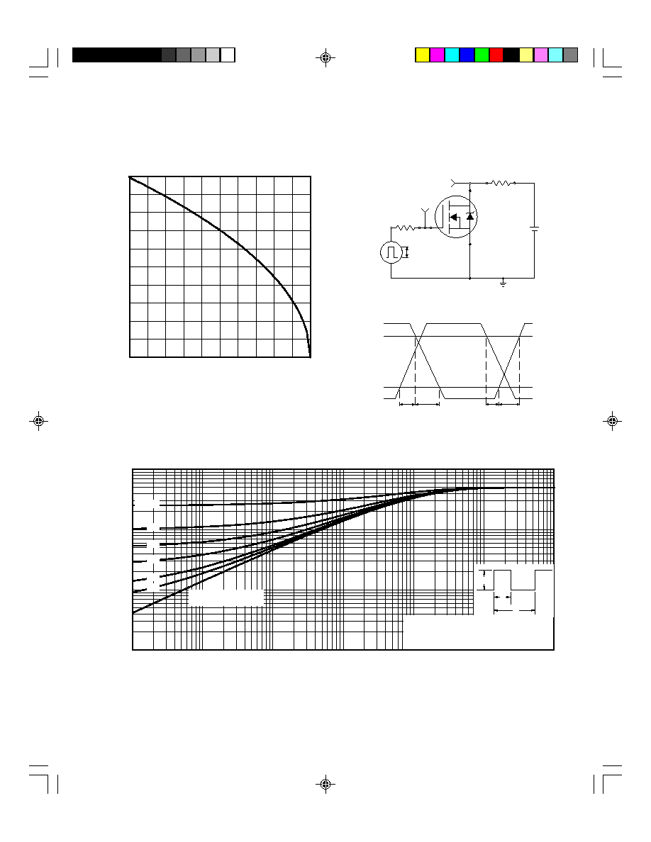
Fig 10a. Switching Time Test Circuit
V
DS
90%
10%
V
GS
t
d(on)
t
r
t
d(off)
t
f
Fig 10b. Switching Time Waveforms
V
DS
Pulse Width
1
µs
Duty Factor
0.1 %
R
D
V
GS
R
G
D.U.T.
10V
+
-
V
DD
Fig 11. Maximum Effective Transient Thermal Impedance, Junction-to-Case
Fig 9. Maximum Drain Current Vs.
Case Temperature
25
50
75
100
125
150
0.0
0.5
1.0
1.5
2.0
2.5
T , Case Temperature ( C)
I , Drain Current (A)
°
C
D
0.01
0.1
1
10
0.00001
0.0001
0.001
0.01
0.1
1
10
Notes:
1. Duty factor D =
t / t
2. Peak T = P
x Z
+ T
1
2
J
DM
thJC
C
P
t
t
DM
1
2
t , Rectangular Pulse Duration (sec)
Thermal Response
(Z )
1
thJC
0.01
0.02
0.05
0.10
0.20
D = 0.50
SINGLE PULSE
(THERMAL RESPONSE)