 | ÐлекÑÑоннÑй компоненÑ: MBR340 | СкаÑаÑÑ:  PDF PDF  ZIP ZIP |
Äîêóìåíòàöèÿ è îïèñàíèÿ www.docs.chipfind.ru
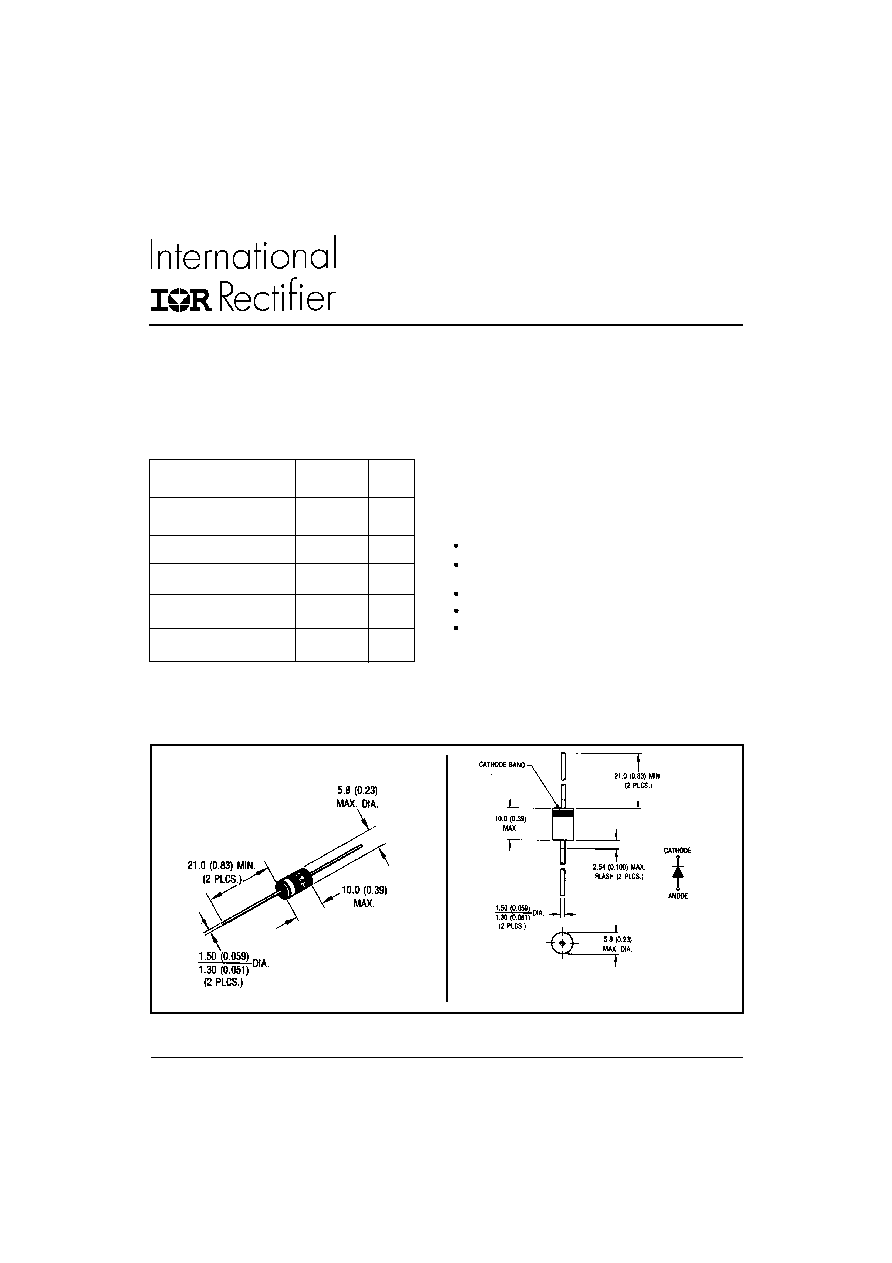
Dimensions in millimeters and inches
Outline C - 16
CASE STYLE AND DIMENSIONS
I
F(AV)
Rectangular
3.0
A
waveform
V
RRM
50/60
V
I
FSM
@ tp = 5 µs sine
460
A
V
F
@
3 Apk, T
J
= 25°C
0.73
V
T
J
- 40 to 150
°C
Characteristics
Units
The MBR350, MBR360 axial leaded Schottky rectifier has
been optimized for very low forward voltage drop, with
moderate leakage. Typical applications are in switching
power supplies, converters, free-wheeling diodes, and
reverse battery protection.
Low profile, axial leaded outline
High purity, high temperature epoxy encapsulation for
enhanced mechanical strength and moisture resistance
Very low forward voltage drop
High frequency operation
Guard ring for enhanced ruggedness and long term
reliability
Description/ Features
Major Ratings and Characteristics
SCHOTTKY RECTIFIER
3.0 Amp
MBR350
MBR360
Bulletin PD-20594 rev. B 03/03
1
www.irf.com
MBR350
MBR360
MBR350, MBR360
Bulletin PD-20594 rev. B 03/03
2
www.irf.com
T
J
Max. Junction Temperature Range(*) -40 to 150
°C
T
stg
Max. Storage Temperature Range
-40 to 150
°C
R
thJL
Typical Thermal Resistance Junction
30
°C/W DC operation (* See Fig. 4)
to Lead
(**)
wt
Approximate Weight
1.2 (0.042) g (oz.)
Case Style
C - 16
I
F(AV)
Max. Average Forward Current
3.0
A
50% duty cycle @ T
L
= 50°C, rectangular wave form
* See Fig. 4
I
FSM
Max. Peak One Cycle Non-Repetitive
460
5µs Sine or 3µs Rect. pulse
Surge Current * See Fig. 6
80
10ms Sine or 6ms Rect. pulse
E
AS
Non-Repetitive Avalanche Energy
5.0
mJ
T
J
= 25 °C, I
AS
= 1 Amps, L = 10 mH
I
AR
Repetitive Avalanche Current
1.0
A
Current decaying linearly to zero in 1 µsec
Frequency limited by T
J
max. V
A
= 1.5 x V
R
typical
Part number
MBR350
MBR360
V
R
Max. DC Reverse Voltage (V)
V
RWM
Max. Working Peak Reverse Voltage (V)
Voltage Ratings
50
60
Thermal-Mechanical Specifications
V
FM
Max. Forward Voltage Drop
0.58
V
@ 1.0A
* See Fig. 1
(1)
0.73
V
@ 3.0A
T
J
= 25 °C
1.06
V
@ 9.4A
0.49
V
@ 1.0A
0.64
V
@ 3.0A
T
J
= 125 °C
0.89
V
@ 9.4A
I
RM
Max. Reverse Leakage Current
0.6
mA
T
J
= 25 °C
* See Fig. 2
(1)
8
mA
T
J
= 100 °C
V
R
= rated V
R
15
mA
T
J
= 125 °C
C
T
Typical Junction Capacitance
190
pF
V
R
= 5V
DC
(test signal range 100Khz to 1Mhz) 25°C
L
S
Typical Series Inductance
9.0
nH
Measured lead to lead 5mm from package body
dv/dt Max. Voltage Rate of Change
10000
V/µs
(Rated V
R
)
Electrical Specifications
(1) Pulse Width < 300µs, Duty Cycle <2%
Parameters
Value
Units
Conditions
Parameters
Value
Units
Conditions
(**) Mounted 1 inch square PCB, thermal probe connected to lead 2mm from package
Absolute Maximum Ratings
Following any rated
load condition and with
rated V
RRM
applied
A
Parameters
Value
Units
Conditions
<
thermal runaway condition for a diode on its own heatsink
(*) dPtot
1
dTj
Rth( j-a)
MBR350, MR360
Bulletin PD-20594 rev. B 03/03
3
www.irf.com
0.001
0.01
0.1
1
10
100
0
20
40
60
125°C
25°C
T = 150°C
J
10
100
1000
0
40
80
120
160
T = 25°C
J
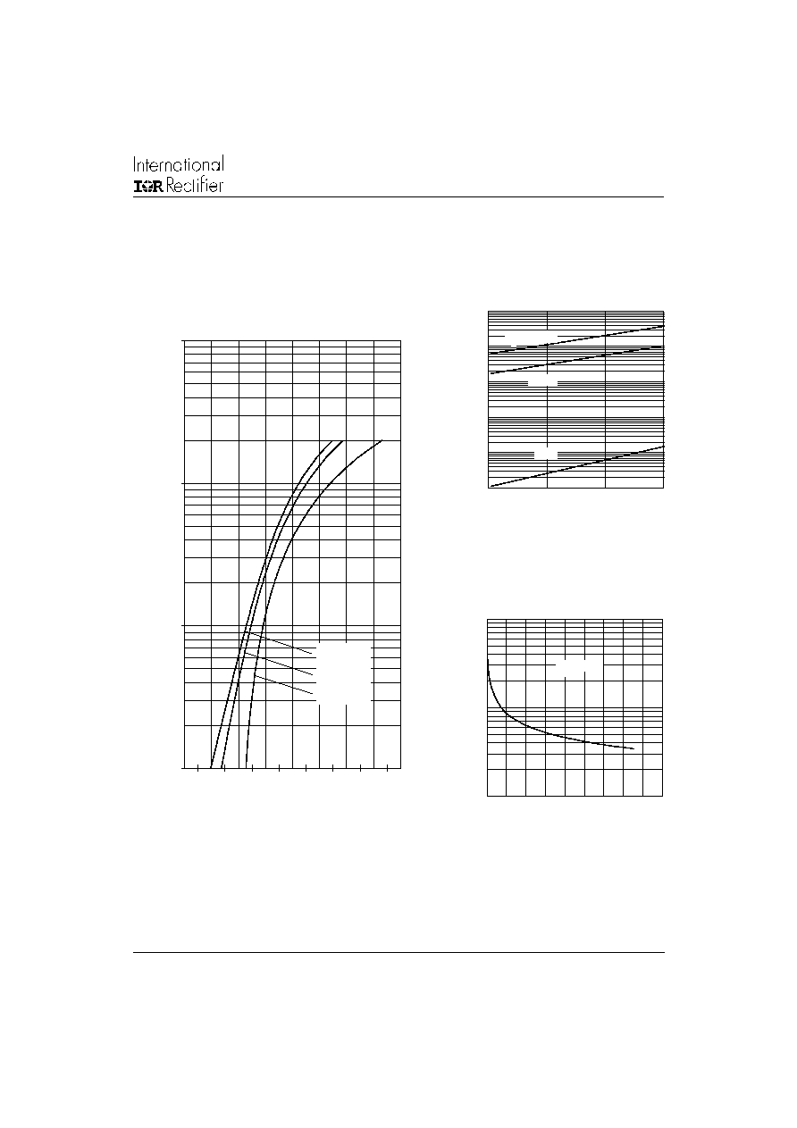
Fig. 1 - Max. Forward Voltage Drop Characteristics
Forward Voltage Drop - V
FM
(V)
Instantaneous Forward Current - I
F
(A)
Reverse Voltage - V
R
(V)
Junction Capacitance - C
T
(pF)
Fig. 3 - Typical Junction Capacitance
Vs. Reverse Voltage
Fig. 2 - Typical Values Of Reverse Current
Vs. Reverse Voltage
Reverse Current - I
R
(mA)
Reverse Voltage - V
R
(V)
0.1
1
10
100
0
0.2
0.4
0.6
0.8
1
1.2
1.4
1.6
Tj = 150°C
Tj = 125°C
Tj = 25°C
MBR350, MBR360
Bulletin PD-20594 rev. B 03/03
4
www.irf.com
Fig. 6 - Max. Non-Repetitive Surge Current
Fig. 5- Forward Power Loss
Characteristics
(2) Formula used: T
C
= T
J
- (Pd + Pd
REV
) x R
thJC
;
Pd = Forward Power Loss = I
F(AV)
x V
FM
@ (I
F(AV)
/
D) (see Fig. 6);
Pd
REV
= Inverse Power Loss = V
R1
x I
R
(1 - D); I
R
@ V
R1
= 80% rated V
R
Fig. 4 - Max. Allowable Lead Temperature
Vs. Average Forward Current
Average Forward Current - I
F(AV)
(A)
Allowable Lead Temperature (°C)
Average Power Loss (Watts)
Average Forward Current - I
F(AV)
(A)
Square Wave Pulse Duration - t
p
(microsec)
Non-Repetitive Surge Current - I
FSM
(A)
0
0.5
1
1.5
2
2.5
3
0 0.5 1 1.5 2 2.5 3 3.5 4 4.5 5
DC
RMS Limit
D = 0.20
D = 0.25
D = 0.33
D = 0.50
D = 0.75
DC
10
100
1000
10
100
1000
10000
At Any Rated Load Condition
And With rated Vrrm Applied
Following Surge
0
20
40
60
80
100
120
140
160
0
1
2
3
4
5
DC
Square wave (D = 0.50)
80% Rated Vr applied
see note (2)

MBR350, MR360
Bulletin PD-20594 rev. B 03/03
5
www.irf.com
Ordering Information Table
Device Code
1
2
3
1
-
Schottky MBR Series
2
-
Current Rating: 3
= 3A
3
-
Voltage Rating
4
-
TR = Tape & Reel package (1200 pcs)
-
= Box package (500 pcs)
MBR
3
60
TR
4
IR WORLD HEADQUARTERS: 233 Kansas St., El Segundo, California 90245, USA Tel: (310) 252-7105
TAC Fax: (310) 252-7309
Visit us at www.irf.com for sales contact information. 03/03
Data and specifications subject to change without notice.
This product has been designed and qualified for Industrial Level.
Qualification Standards can be found on IR's Web site.
40 = 40V
60 = 60V