 | ÐлекÑÑоннÑй компоненÑ: MBRS120 | СкаÑаÑÑ:  PDF PDF  ZIP ZIP |
Äîêóìåíòàöèÿ è îïèñàíèÿ www.docs.chipfind.ru
SCHOTTKY RECTIFIER
1 Amp
MBRS120
Bulletin PD-20644 rev. D 03/03
1
Major Ratings and Characteristics
I
F(AV)
Rectangular
1.0
A
waveform
V
RRM
20
V
I
FSM
@ t
p
= 5 µs sine
310
A
V
F
@
1.0Apk, T
J
= 125°C
0.35
V
T
J
range
- 65 to 150
°C
Characteristics
MBRS120 Units
The MBRS120 surface-mount Schottky rectifier has been
designed for applications requiring low forward drop and
small foot prints on PC boards. Typical applications are in disk
drives, switching power supplies, converters, free-wheeling
diodes, battery charging, and reverse battery protection.
Small foot print, surface mountable
Very low forward voltage drop
High frequency operation
Guard ring for enhanced ruggedness and long term
reliability
Description/Features
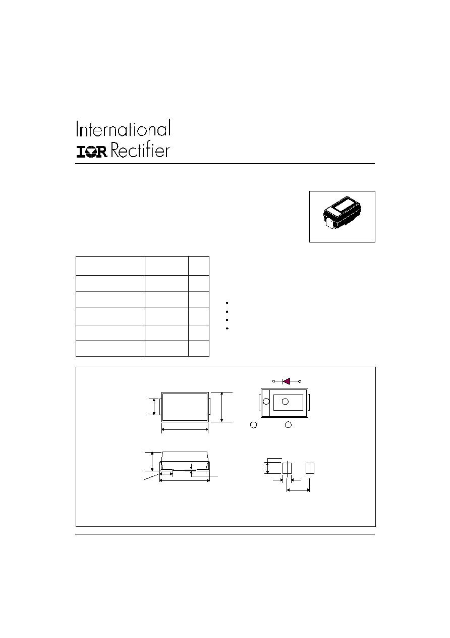
SMB
3.80 (.150)
3.30 (.130)
4.70 (.185)
4.10 (.161)
2.15 (.085)
1.80 (.071)
2.40 (.094)
1.90 (.075)
1.30 (.051)
0.76 (.030)
0.30 (.012)
0.15 (.006)
5.60 (.220)
5.00 (.197)
4.0 (.157)
2.0 TYP.
(.079 TYP.)
2.5 TYP.
(.098 TYP.)
SOLDERING PAD
CATHODE
ANODE
1
2
1
2
POLARITY
PART NUMBER
4.2 (.165)
Outline SMB
Dimensions in millimeters and (inches)
For recommended footprint and soldering techniques refer to application note #AN-994
Device Marking: IR12
www.irf.com
MBRS120
Bulletin PD-20644 rev. D 03/03
2
www.irf.com
V
R
Max. DC Reverse Voltage (V)
V
RWM
Max. Working Peak Reverse Voltage (V)
20
Voltage Ratings
Part number
MBRS120
V
FM
Max. Forward Voltage Drop (1)
0.42
0.45
V
@ 1A
0.46
0.52
V
@ 2A
0.33
0.37
V
@ 1A
0.39
0.45
V
@ 2A
0.30
0.35
V
@ 1A
0.36
0.43
V
@ 2A
I
RM
Max. Reverse Leakage Current (1)
0.015
0.2
mA
T
J
= 25 °C
2.0
6.0
mA
T
J
= 100 °C
V
R
= rated V
R
7.0
20
mA
T
J
= 125 °C
C
T
Typical Junction Capacitance
110
-
pF
V
R
= 5V
DC
(test signal range 100kHz to
1Mhz), @ 25°C
L
S
Typical Series Inductance
2.0
-
nH
Measured lead to lead 5mm from package body
dv/dt Max. Voltage Rate of Change
-
10000
V/ µs
(Rated V
R
)
T
J
= 25 °C
T
J
= 100 °C
Electrical Specifications
Parameters
Typ.
Max.
Units
Conditions
(1) Pulse Width < 300µs, Duty Cycle < 2%
T
J
= 125 °C
T
J
Max. Junction Temperature Range (*) - 65 to 150
°C
T
stg
Max. Storage Temperature Range
- 65 to 150
°C
R
thJL
Max. Thermal Resistance Junction
30
°C/W DC operation
to Lead
(**)
R
thJA
Max. Thermal Resistance Junction
80
°C/W
to Ambient
Wt
Approximate Weight
0.10(0.003) gr (oz)
Case Style
SMB
Similar DO-214AA
Device Marking
IR12
Parameters
Value
Units
Conditions
<
thermal runaway condition for a diode on its own heatsink
(**) Mounted 1 inch square PCB
Thermal-Mechanical Specifications
(*) dPtot
1
dTj
Rth( j-a)
I
F(AV)
Max. Average Forward Current
1.0
A
50% duty cycle @ T
L
= 138°C, rectangular wave form
I
FSM
Max. Peak One Cycle Non-Repetitive
310
5µs Sine or 3µs Rect. pulse
Surge Current
40
10ms Sine or 6ms Rect. pulse
E
AS
Non Repetitive Avalanche Energy
2.0
mJ
T
J
= 25 °C, I
AS
= 1A, L = 4mH
I
AR
Repetitive Avalanche Current
0.8
A
Current decaying linearly to zero in 1 µsec
Frequency limited by T
J
max. Va = 1.5 x Vr typical
Parameters
Value Units Conditions
Absolute Maximum Ratings
Following any rated
load condition and
with rated V
RRM
applied
MBRS120
Bulletin PD-20644 rev. D 03/03
3
www.irf.com
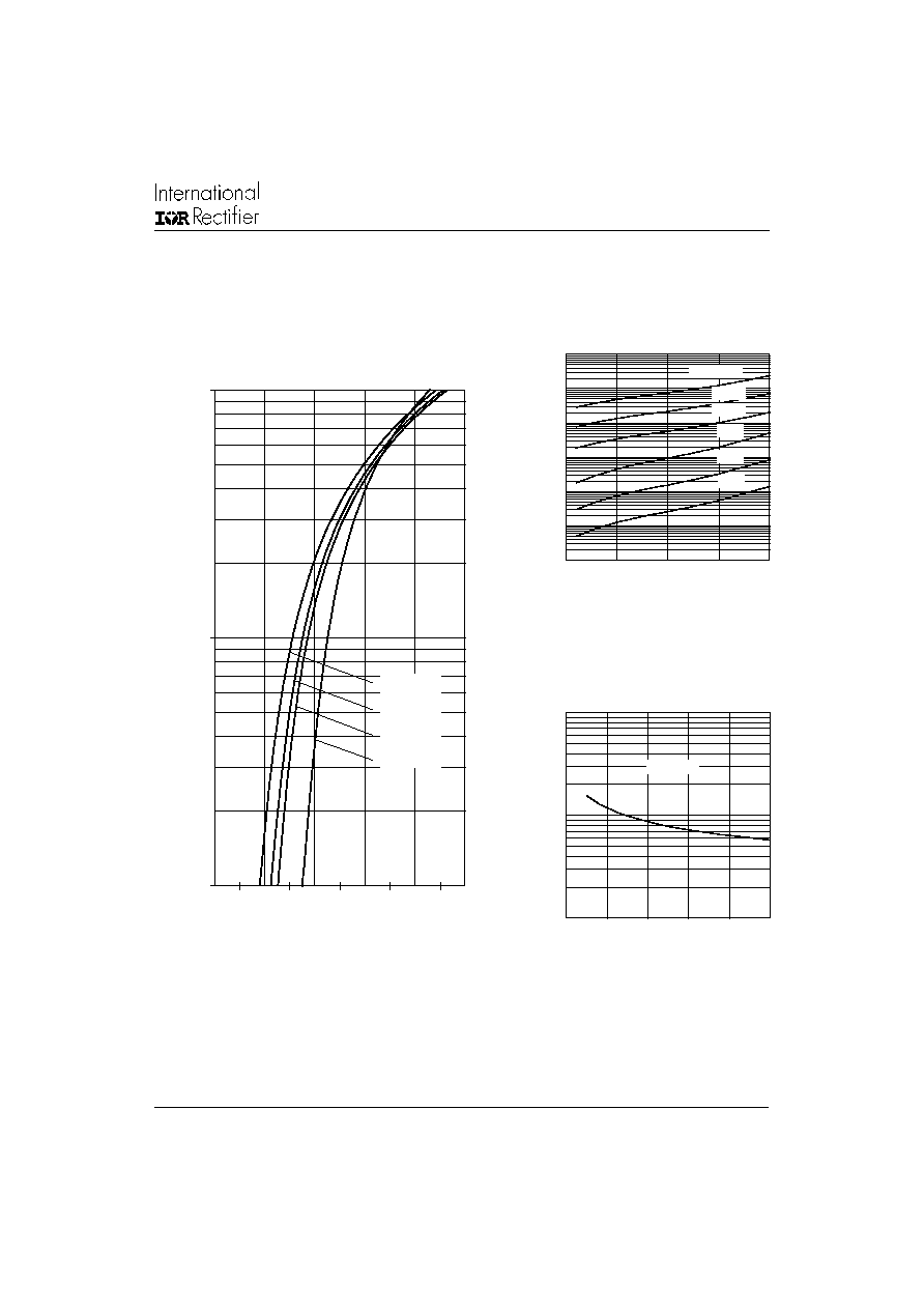
Fig. 2 - Typical Peak Reverse Current
Vs. Reverse Voltage
Fig. 3 - Typical Junction Capacitance
Vs. Reverse Voltage
Fig. 1 - Maximum Forward Voltage Drop Characteristics
Instantaneous Forward Current - I
F
(A)
Forward Voltage Drop - V
FM
(V)
Reverse Voltage - V
R
(V)
Reverse Current - I
R
(mA)
Reverse Voltage - V
R
(V)
Junction Capacitance - C
T
(pF)
0.1
1
10
0
0.2
0.4
0.6
0.8
1
Tj = 150°C
Tj = 125°C
Tj = 100°C
Tj = 25°C
0.0001
0.001
0.01
0.1
1
10
100
0
5
10
15
20
125°C
100°C
75°C
50°C
25°C
Tj = 150°C
10
100
1000
0
4
8
12
16
20
Tj = 25°C
MBRS120
Bulletin PD-20644 rev. D 03/03
4
www.irf.com
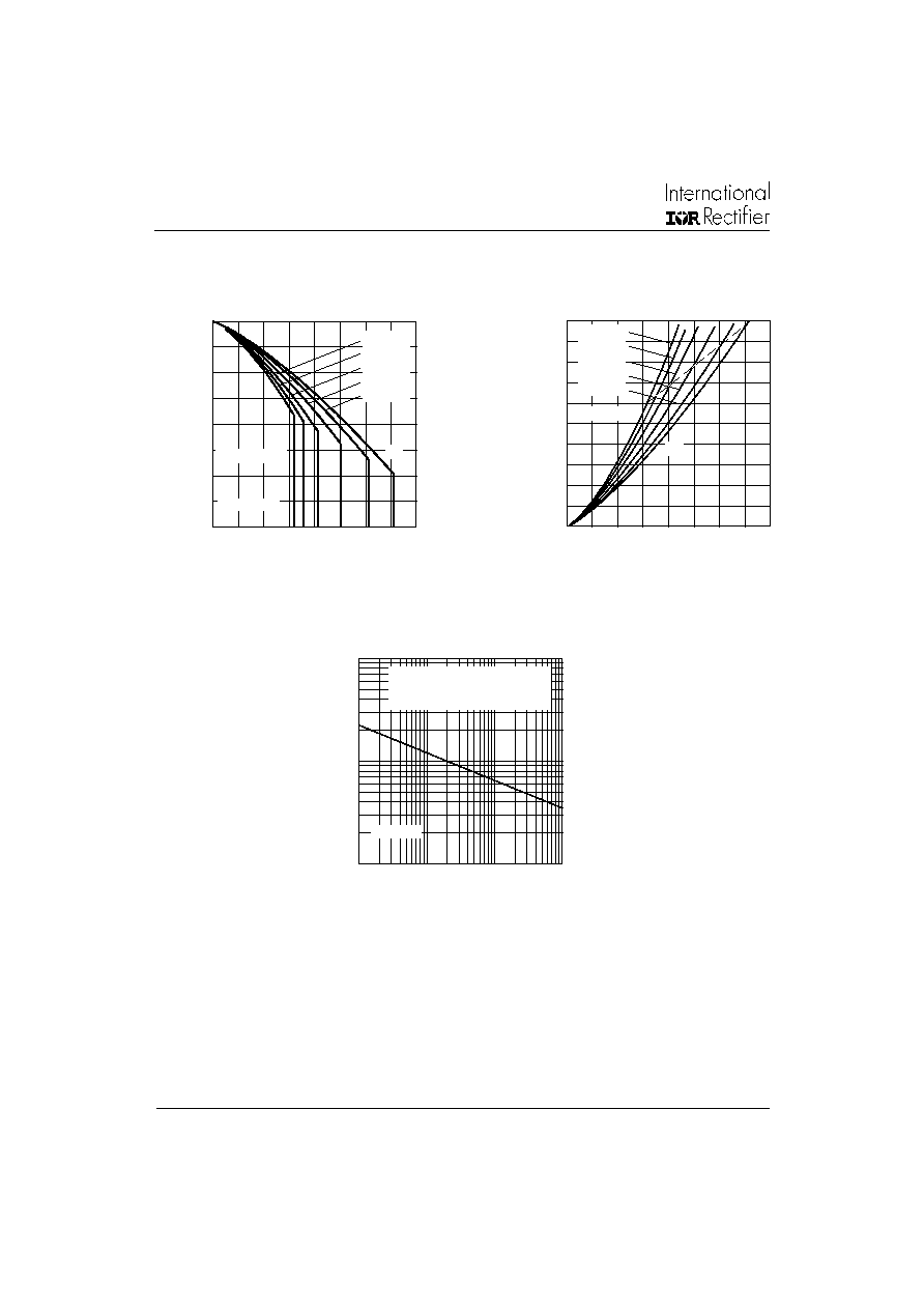
Fig. 4 - Maximum Average Forward Current
Vs. Allowable Lead Temperature
Fig. 6 - Maximum Peak Surge Forward Current Vs. Pulse Duration
(2) Formula used: T
C
= T
J
- (Pd + Pd
REV
) x R
thJC
;
Pd = Forward Power Loss = I
F(AV)
x V
FM
@ (I
F(AV)
/
D) (see Fig. 6);
Pd
REV
= Inverse Power Loss = V
R1
x I
R
(1 - D)
Average Forward Current - I
F(AV)
(A)
Allowable Lead Temperature (°C)
Average Forward Current - I
F(AV)
(A)
Allowable Power Loss (Watts)
Square Wave Pulse Duration - t
p
(microsec)
Non-Repetitive Surge Current - I
FSM
(A)
130
135
140
145
150
0
0.2 0.4 0.6 0.8
1
1.2 1.4 1.6
DC
see note (2)
Square wave
D = 0.20
D = 0.25
D = 0.33
D = 0.50
D = 0.75
0
0.1
0.2
0.3
0.4
0.5
0
0.4
0.8
1.2
1.6
DC
RMS Limit
D = 0.20
D = 0.25
D = 0.33
D = 0.50
D = 0.75
10
100
1000
10
100
1000
10000
Tj = 25°C
At Any Rated Load Condition
And With Rated Vrrm Applied
Following Surge
Fig. 5 - Maximum Average Forward Dissipation
Vs. Average Forward Current
MBRS120
Bulletin PD-20644 rev. D 03/03
5
www.irf.com
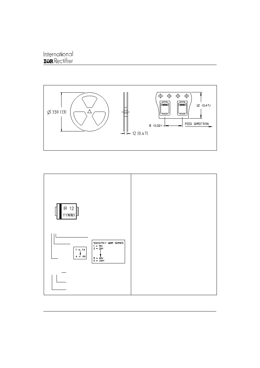
IR LOGO
YEAR
CURRENT
IR12
VOLTAGE
YYWWX
WEEK
SITE ID
Tape & Reel Information
Dimensions in millimetres and (inches)
Marking & Identification
Ordering Information
MBRS120TR - TAPE AND REEL
WHEN ORDERING, INDICATE THE PART
NUMBER AND THE QUANTITY ( IN MULTIPLES OF
3000 PIECES).
EXAMPLE:
MBRS120TR - 6000 PIECES
Each device has 2 rows for identification. The first row
designates the device as manufactured by International
Rectifier as indicated by the letters "IR", and the Part
Number (indicates the current and the voltage rating).
The second row indicates the year, the week of
manufacturing and the Site ID.