Äîêóìåíòàöèÿ è îïèñàíèÿ www.docs.chipfind.ru
1
MUR1020CT
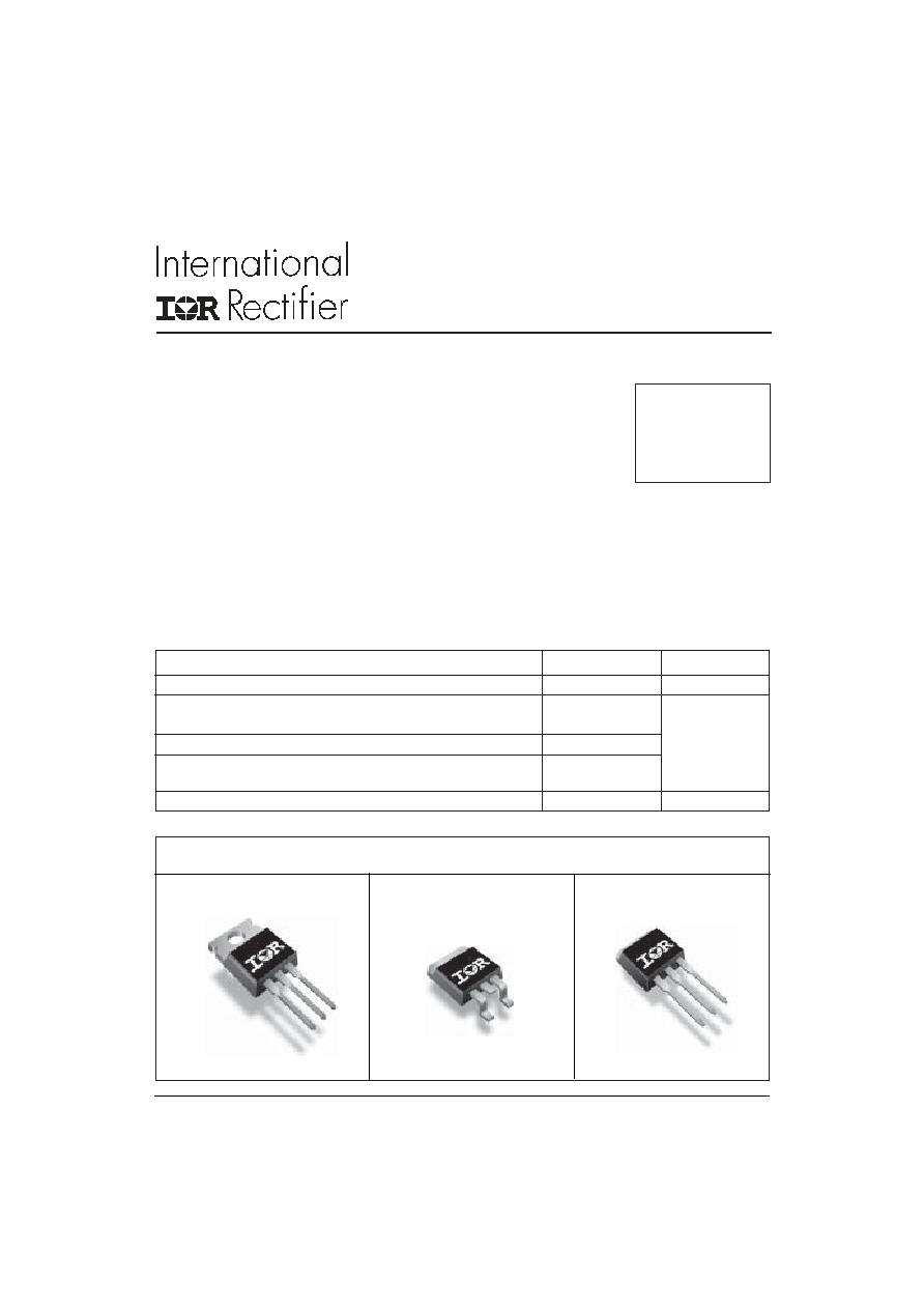
TO-220AB
Case Styles
MURB1020CT
D
2
PAK
MURB1020CT-1
TO-262
MUR1020CT
MURB1020CT
MURB1020CT-1
Bulletin PD-20738 rev. B 12/03
t
rr
= 25ns
I
F(AV)
= 10Amp
V
R
= 200V
· Ultrafast Recovery Time
· Low Forward Voltage Drop
· Low Leakage Current
· 175°C Operating Junction Temperature
Features
Description/ Applications
International Rectifier's MUR.. series are the state of the art Ultra fast recovery rectifiers specifically designed with
optimized performance of forward voltage drop and ultra fast recovery time.
The planar structure and the platinum doped life time control, guarantee the best overall performance, ruggedness and
reliability characteristics.
These devices are intended for use in the output rectification stage of SMPS, UPS, DC-DC converters as well as free-
wheeling diode in low voltage inverters and chopper motor drives.
Their extremely optimized stored charge and low recovery current minimize the switching losses and reduce over
dissipation in the switching element and snubbers.
Absolute Maximum Ratings
Ultrafast Rectifier
V
RRM
Peak Repetitive Peak Reverse Voltage
200
V
I
F(AV)
Average Rectified Forward Current
Per Leg
5
A
Total Device, (Rated V
R
), T
C
= 149°C
Total Device
10
I
FSM
Non Repetitive Peak Surge Current
Per Leg
50
I
FM
Peak Repetitive Forward Current
Per Leg
10
(Rated V
R
, Square wave, 20 KHz), T
C
= 149°C
T
J
,
T
STG
Operating Junction and Storage Temperatures
- 65 to 175
°C
Parameters
Max
Units
www.irf.com
MUR1020CT, MURB1020CT, MURB1020CT-1
Bulletin PD-20738 rev. B 12/03
2
www.irf.com
V
BR
,
V
r
Breakdown Voltage,
200
-
-
V
I
R
= 100µA
Blocking Voltage
V
F
Forward Voltage
-
0.87 0.99
V
I
F
= 5A, T
J
= 125°C
-
1.02 1.20
V
I
F
= 10A, T
J
= 125°C
-
1.12 1.25
V
I
F
= 10A, T
J
= 25°C
I
R
Reverse Leakage Current
-
-
10
µA
V
R
= V
R
Rated
-
-
250
µA
T
J
= 150°C, V
R
= V
R
Rated
C
T
Junction Capacitance
-
8
-
pF
V
R
= 200V
L
S
Series Inductance
-
8.0
-
nH
.
Electrical Characteristics @ T
J
= 25°C (unless otherwise specified)
Parameters
Min Typ Max Units Test Conditions
Measured lead to lead 5mm from package body
t
rr
Reverse Recovery Time
-
-
35
ns
I
F
= 1.0A, di
F
/dt = 50A/µs, V
R
= 30V
-
-
25
I
F
= 0.5A, I
R
= 1.0A, I
REC
= 0.25A
-
24
-
T
J
= 25°C
35
T
J
= 125°C
I
RRM
Peak Recovery Current
-
3.3
-
A
T
J
= 25°C
-
5.0
-
T
J
= 125°C
Q
rr
Reverse Recovery Charge
-
33
-
nC
T
J
= 25°C
-
76
-
T
J
= 125°C
Dynamic Recovery Characteristics @ T
J
= 25°C (unless otherwise specified)
I
F
= 5A
V
R
= 160V
di
F
/dt = 200A/µs
Parameters
Min Typ Max Units Test Conditions
Parameters
Min
Typ
Max
Units
T
J
Max. Junction Temperature Range
-
-
- 65 to 175
°C
T
Stg
Max. Storage Temperature Range
-
-
- 65 to 175
R
thJC
Thermal Resistance, Junction to Case
Per Leg
-
-
5
°C/W
R
thJA
Thermal Resistance, Junction to Ambient
Per Leg
-
-
50
R
thCS
Thermal Resistance, Case to Heatsink
-
0.5
-
Wt
Weight
-
2.0
-
g
-
0.07
-
(oz)
Mounting Torque
6.0
-
12
Kg-cm
5.0
-
10
lbf.in
Thermal - Mechanical Characteristics
Mounting Surface, Flat, Smooth and Greased
Bulletin PD-20738 rev. B 12/03
3
MUR1020CT, MURB1020CT, MURB1020CT-1
www.irf.com
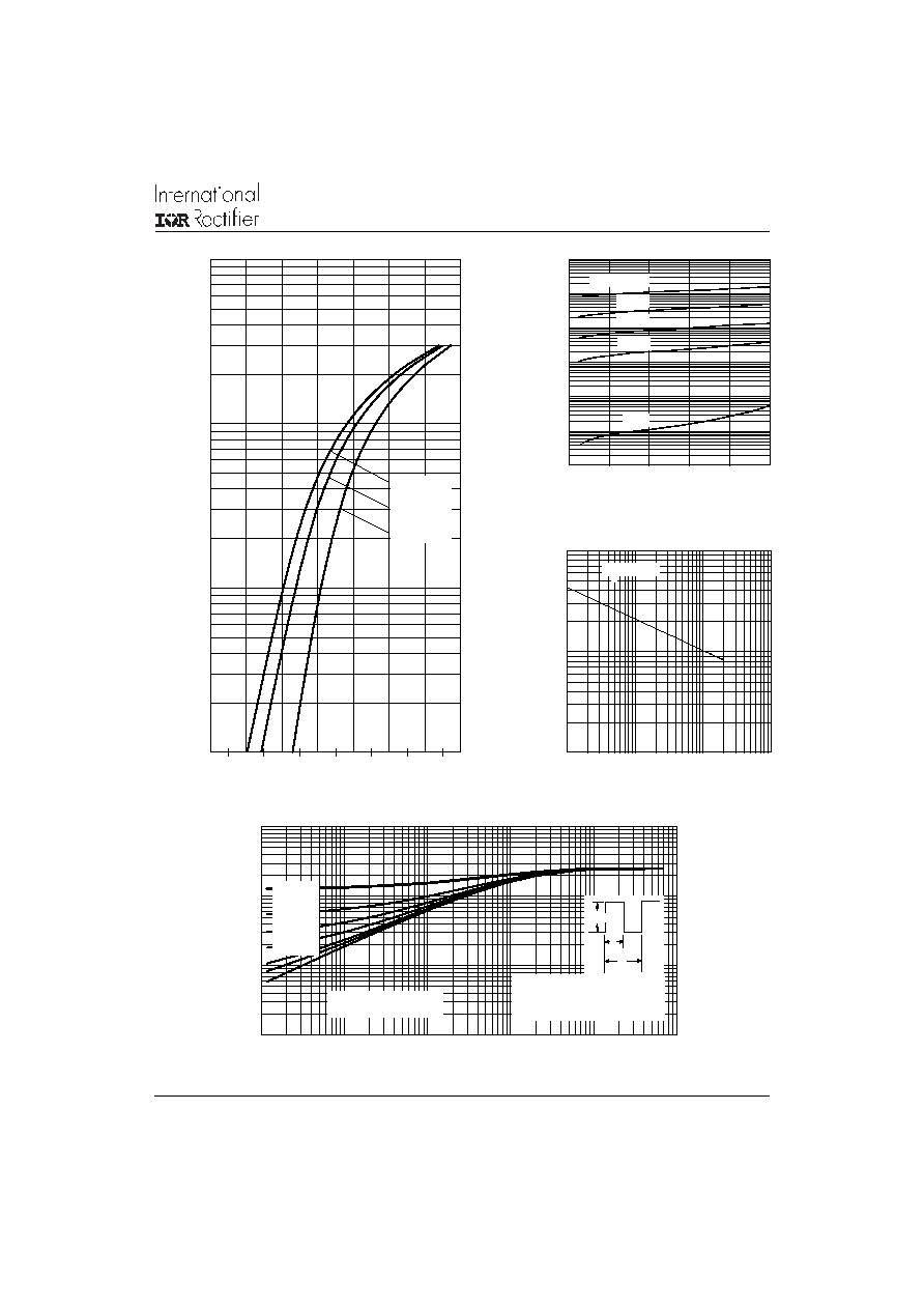
Fig. 2 - Typical Values Of Reverse Current
Vs. Reverse Voltage
Fig. 1 - Typical Forward Voltage Drop Characteristics
Reverse Voltage - V
R
(V)
Fig. 3 - Typical Junction Capacitance
Vs. Reverse Voltage
Forward Voltage Drop - V
FM
(V)
Instantaneous Forward Current - I
F
(A)
Reverse Current - I
R
(µA)
Reverse Voltage - V
R
(V)
Junction Capacitance - C
T
(pF)
Fig. 4 - Max. Thermal Impedance Z
thJC
Characteristics
t
1
, Rectangular Pulse Duration (Seconds)
Thermal Impedance Z
thJC
(°C/W)
0.0001
0.001
0.01
0.1
1
10
100
0
40
80
120
160
200
125°C
100°C
25°C
T = 175°C
150°C
J
1
10
100
1
10
100
1000
T = 25°C
J
0.1
1
10
100
0.2
0.4
0.6
0.8
1
1.2
1.4
1.6
T = 175°C
T = 125°C
T = 25°C
J
J
J
0.01
0.1
1
10
0.00001
0.0001
0.001
0.01
0.1
1
Single Pulse
(Thermal Resistance)
D = 0.50
D = 0.20
D = 0.10
D = 0.05
D = 0.02
D = 0.01
2
t
1
t
P
DM
Notes:
1. Duty factor D = t1/ t2
2. Peak Tj = Pdm x ZthJC + Tc
MUR1020CT, MURB1020CT, MURB1020CT-1
Bulletin PD-20738 rev. B 12/03
4
www.irf.com
(2) Formula used: T
C
= T
J
- (Pd + Pd
REV
) x R
thJC
;
Pd = Forward Power Loss = I
F(AV)
x V
FM
@ (I
F(AV)
/
D) (see Fig. 6);
Pd
REV
= Inverse Power Loss = V
R1
x I
R
(1 - D); I
R
@ V
R1
= rated V
R
Fig. 5 - Max. Allowable Case Temperature
Vs. Average Forward Current
Fig. 6 - Forward Power Loss Characteristics
Average Power Loss ( Watts )
trr ( ns )
Qrr ( nC )
Average Forward Current - I
F
(AV)
(A)
Allowable Case Temperature (°C)
Average Forward Current - I
F
(AV)
(A)
Fig. 8 - Typical Stored Charge vs. di
F
/dt
Fig. 7 - Typical Reverse Recovery vs. di
F
/dt
di
F
/dt (A/µs )
di
F
/dt (A/µs )
0
1
2
3
4
5
6
7
0
1
2
3
4
5
6
7
8
DC
RMS Limit
D = 0.01
D = 0.02
D = 0.05
D = 0.1
D = 0.2
D = 0.5
10
20
30
40
50
100
1000
I
F
= 10 A
I
F
= 5 A
V = 160V
T = 125°C
T = 25°C
R
J
J
0
20
40
60
80
100
120
140
160
100
1000
I
F
= 10 A
I
F
= 5 A
V = 160V
T = 125°C
T = 25°C
R
J
J
130
140
150
160
170
180
0
2
4
6
8
DC
Square wave (D = 0.50)
Rated Vr applied
see note (2)
Bulletin PD-20738 rev. B 12/03
5
MUR1020CT, MURB1020CT, MURB1020CT-1
www.irf.com
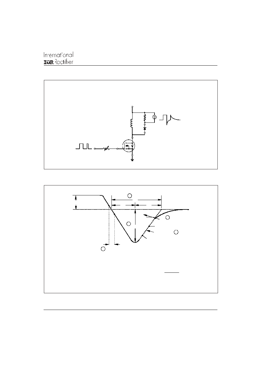
Fig. 10 - Reverse Recovery Waveform and Definitions
IRFP250
D.U.T.
L = 70µH
V = 200V
R
0.01
G
D
S
dif/dt
ADJUST
t
a
t
b
t
rr
Q
rr
I
F
I
RRM
I
RRM
0.5
di(rec)M/dt
0.75 I
RRM
5
4
3
2
0
1
di /dt
f
Fig. 9- Reverse Recovery Parameter Test Circuit
Reverse Recovery Circuit
di
F
/dt
di
F
/dt
4. Q
rr
- Area under curve defined by t
rr
and I
RRM
5. di (rec) M / dt - Peak rate of change of
current during t b portion of t rr
1. di
F
/dt - Rate of change of current through zero
crossing
2. I
RRM
- Peak reverse recovery current
3. t
rr
- Reverse recovery time measured from zero
crossing point of negative going I
F
to point where
a line passing through 0.75 I
RRM
and 0.50 I
RRM
extrapolated to zero current
Q rr =
t rr x I RRM
2