 | ÐлекÑÑоннÑй компоненÑ: PVA1352 | СкаÑаÑÑ:  PDF PDF  ZIP ZIP |
PVA13
PD 1.020D
Series PVA13
Microelectronic
Power IC Relay
Single-Pole, 300mA, 0-100V AC/DC
BOSFET
®
Photovoltaic Relay
General Description
The Photovoltaic AC Relay (PVA) is a single-pole,
normally open solid state replacement for electro-
mechanical relays used for general purpose switching of
analog signals. It utilizes as an output switch a unique
bidirectional (AC or DC) MOSFET power IC termed a
BOSFET. The BOSFET is controlled by a photovoltaic
generator of novel construction, which is energized by
radiation from a dielectrically isolated light emitting diode
(LED).
The PVA overcomes the limitations of both conventional
and reed electromechanical relays by offering the solid
state advantages of long life, high operating speed, low
pick-up power, bounce-free operation, low thermal
voltages and miniaturization. These advantages allow
product improvement and design innovations in many
applications such as process control, multiplexing,
telecommunications, automatic test equipment and data
acquisition.
The PVA can switch analog signals from thermocouple
level to 100 volts peak AC or DC polarity. Signal frequen-
cies into the RF range are easily controlled and switching
rates up to 2kHz are achievable. The extremely small
thermally generated offset voltages allow increased
measurement accuracies.
Unique silicon technology developed by International
Rectifier forms the heart of the PVA. The monolithic
BOSFET contains a bidirectional N-channel power
MOSFET output structure. In addition, this power IC chip
has input circuitry for fast turn-off and gate protection
functions. This section of the BOSFET chip utilizes both
bipolar and MOS technology to form NPN transistors, P-
channel MOSFETs, resistors, diodes and capacitors.
The photovoltaic generator similarly utilizes a unique
International Rectifier alloyed multijunction structure. The
excellent current conversion efficiency of this technique
results in the very fast response of the PVA microelec-
tronic power IC relay.
This advanced semiconductor technology has created a
radically new control device. Designers can now develop
switching systems to new standards of electrical perfor-
mance and mechanical compactness.
PVA13 Features
BOSFET Power IC
n
10
10
Operations
n
300µsec Operating Time
n
0.2µVolt Thermal Offset
n
3 milliwatts Pick-Up Power
n
1000V/µsec dv/dt
n
Bounce-Free
n
8-pin DIP Package
n
-40°C to 85°C
n
UL recognized
n
Part Identification
Part Number
Operating
Sensitivity
Off-State
Voltage (AC/DC)
Resistance
PVA1352
10
8
Ohms
0 100V
5 mA
PVA1354
10
10
Ohms
(BOSFET is a trademark of International Rectifier)
Series PVA13 BOSFET
®
Photovoltaic Relay
INPUT CHARACTERISTICS
PVA1352
PVA1354
Units
Minimum Control Current
(see figures 1 and 2)
DC
For 200mA Continuous Load Current
2.0
mA@25°C
For 250mA Continuous Load Current
5.0
mA@40°C
For 125mA Continuous Load Current
5.0
mA@85°C
Maximum Control Current for Off-State Resistance at 25°C
10
µA(DC)
Control Current Range (Caution: current limit input LED. See figure 6)
2.0 to 25
mA(DC)
Maximum Reverse Voltage
7.0
V(DC)
Electrical Specifications (-40
°
C
T
A
+85
°
C unless otherwise specified
)
GENERAL CHARACTERISTICS (PVA1352 and PVA1354)
Units
Dielectric Strength: Input-Output
2500
V
RMS
Insulation Resistance: Input-Output @ 90V
DC
10
12
@ 25°C - 50% RH
Maximum Capacitance: Input-Output
1.0
pF
Max. Pin Soldering Temperature
(1.6mm below seating plane, 10 seconds max.)
+260
Ambient Temperature Range:
Operating
-40 to +85
°
C
Storage
-40 to +100
OUTPUT CHARACTERISTICS
PVA1352
PVA1354
Units
Operating Voltage Range
0 to ± 100
V
(peak)
Maxiumum Load Current 40°C
(see figures 1and 2)
315
mA
(DC)
Response Time @25°C
(see figures 7 and 8)
Maximum T(on) @ 12mA Control, 50 mA Load, 50 VDC
300
µs
Maximum T(off) @ 12mA Control, 50 mA Load, 50 VDC
50
µs
Maximum On-state Resistance 25°C
(Pulsed) (figure 4) 50 mA Load, 5mA Control
5
Minimum Off-state Resistance 25°C @ 80 VDC
(see figure 5)
10
8
10
10
Maximum Thermal Offset Voltage @ 5.0mA Control
0.2
µvolts
Minimum Off-State dv/dt
1000
V/µs
Output Capacitance
(see figure 9)
15
pF @ 50VDC
Series PVA13 BOSFET
®
Photovoltaic Relay
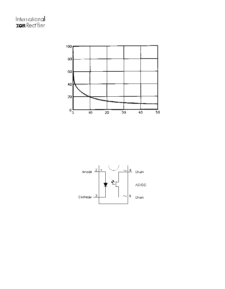
Max. Load Current (mA)
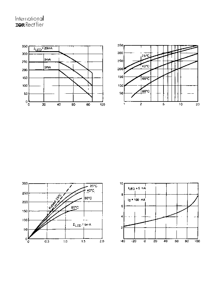
Figure 1. Current Derating Curves
Figure 2. Typical Control Current Requirements
Figure 3.Typical On Characteristics
Figure 4. Typical On-Resistance
R
DD(on)
(
)
ILED (mA)
Ambient Temperature (°C)
Max. Load Current (mA)
Ambient Temperature (°C)
VDD (volts)
Load Current (mA)
Series PVA13 BOSFET
®
Photovoltaic Relay
I D
Of
f
/
I D
Of
f 25°C
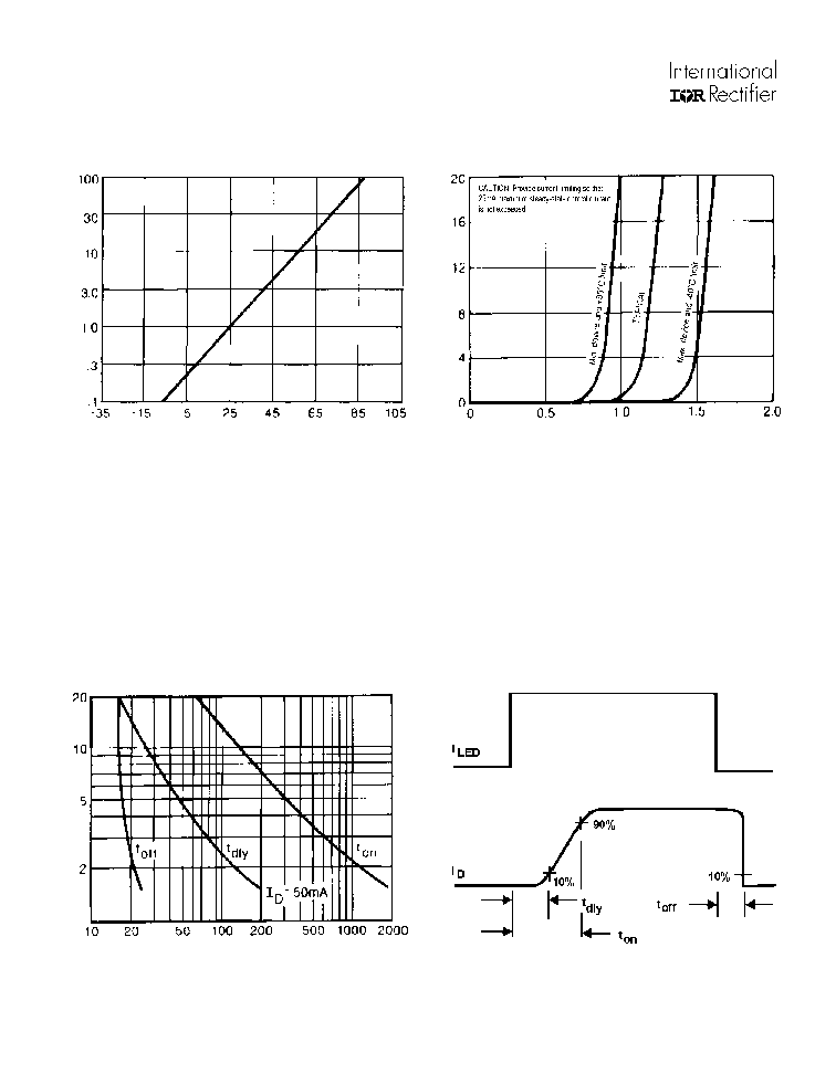
Figure 5. Normalized Off-State Leakage
Figure 6. Input Characteristics
(Current Controlled)
Figure 7.Typical Delay Times
Figure 8. Delay Time Definitions
LED Forward Voltage Drop (Volts DC)
Input Current (mA)
Ambient Temperature (°C)
I LED
(mA)
Delay Time (microseconds)
Series PVA13 BOSFET
®
Photovoltaic Relay
Figure 9. Typical Output Capacitance
T
ypical Capacitance (picofarads)
VDD Drain to Drain Voltage
Wiring Diagram