 | ÐлекÑÑоннÑй компоненÑ: PVAZ172NS | СкаÑаÑÑ:  PDF PDF  ZIP ZIP |
/home/web/doc/html/irf/194462
Data Sheet No. PD 10040C
PVAZ172N
Microelectronic Power IC
HEXFET
®
Power MOSFET Photovoltaic Relay
Single Pole, Normally Open
0-60V AC, 1.0A
General Description
The PVAZ172N Photovoltaic Relay is a single-pole,
normally open solid state relay that can replace elec-
tromechanical relays used for general purpose switch-
ing of DC and AC loads. It utilizes International Rectifier's
HEXFET power MOSFETs as the output switches,
driven by an integrated circuit photovoltaic generator
of novel construction. The output switch is controlled
by radiation from a GaAlAs light emitting diode (LED)
which is optically isolated from the photovoltaic gen-
erator.
These units overcome the limitations of both electro-
mechanical and reed relays by offering the solid-state
advantages of high sensitivity, miniaturization, no con-
tact bounce, long operational life, insensitivity to exter-
nal magnetic fields, shock and vibration, and high reli-
ability inherent with solid state technology. They are
ideally suited for switching high currents or low level
signals without distortion or injection of electrical noise.
These relays are packaged in 8-pin, molded DIP pack-
ages and available with either through-hole or surface-
mount ("gull-wing") leads, in plastic shipping tubes.
Applications
§
Portable Electronics
§
Programmable Logic Controllers
§
Computers and Peripheral Devices
§
Audio Equipment
§
Power Supplies and Power Distribution
§
Instrumentation
(HEXFET is the registered trademark for International Rectifier Power MOSFETs)
Part Identification
PVAZ172N
through-hole
PVAZ172NS
surface-mount (gull-wing)
Features
§
500m
On-Resistance
§
Bounce-Free Operation
§
1.0 Amp capacity
§
4,000 V
RMS
I/O Isolation
§
Solid-State Reliability
§
UL recognized
§
ESD Tolerance:
4000V Human Body Model
500V Machine Model
PVAZ172N
2
www.irf.com
Electrical Specifications (-40°C
T
A
=+85°C unless otherwise specified
)
INPUT CHARACTERISTICS
Limits
Units
Min. Control Current
(see figures 1 and 2)
10
mA
Max. Control Current for Off-State Resistance
@ T
A
=+25°C
0.4
mA
Control Current Range
(Caution: Current limit input LED, see figure 6)
5.0 to 25
mA
Maximum Reverse Voltage
7.0
V
OUTPUT CHARACTERISTICS
Operating Voltage Range
0 to 60
V(AC peak)
Maximum Load Current 40
°
C
(see figures 1 and 2)
1.0
A (DC)
Maximum Pulsed Load Current
@T
A
=+25°C (100 ms @ 10% duty cycle)
2.4
A (AC peak)
Maximum Turn-On Time
@T
A
=+25°C (see figure 7)
2.0
ms
For 500mA, 50VDC Load, 10mA Control
Maximum Turn-Off Time
@TA=+25°C (see figure 7)
0.5
ms
For 500mA, 50VDC Load, 10mA Control
Maximum On State Resistance
@TA=+25°C(pulsed) (See figure 4)
500
m
1.0A Load, 10mA Control
Minimum Off State Resistance @T
A
=+25°C @ 48 VDC (see fig
ure
5)
10
8
Ohms
Minimum Off-State dv/dt
1000
V/
µ
s
Output Capacitance
(see figure 9)
150
pF @ 50 VDC
GENERAL CHARACTERISTICS
Limits
Units
Dielectric Strength, Input-Output
4000
V
(RMS)
Insulation Resistance, Input-Output , 90 V
DC
10
12
@T
A
=+25°C - 50% RH
Capacitance, Input-Output
1.0
pF
Lead Temperature (1.6mm below seating plane) for 10 seconds
+260
°C
Ambient Temperature Range:
Operating
-40 to +85
°C
Storage
-40 to +100
°C
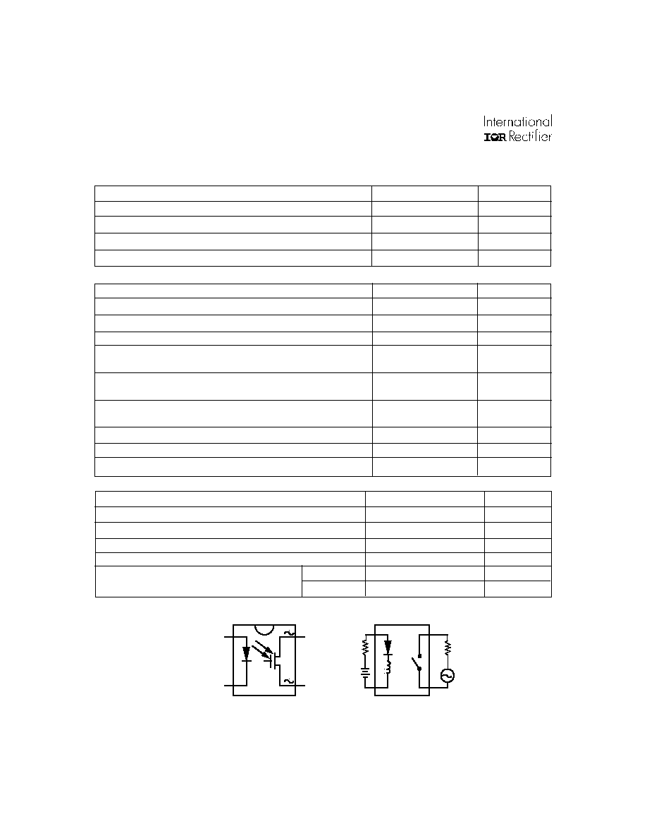
Wiring Diagrams:
Electromechanical
Analogy
5
2
3
8
+
Anode
Cathode
Drain
Schematic
Drain
2
3
8
5
+
PVAZ172N
www.irf.com
3
In
p
u
t C
u
r
r
e
n
t (
m
A
)
LED Forward Voltage Drop (Volts DC)
16
20
12
8
4
0
0.5
1.0
1.5
2.0
0
CAUTION: provide current limiting
so that 25 mA maximum steady-
state control current rating is
not exceeded
TY
P
IC
A
L
M
i
n
.
d
e
v
ic
e
an
d
+
8
5 de
g. C
lim
it
M
ax.
dev
i
ce a
nd -4
0
d
eg
. C
lim
it
Ambient Temperature (deg. C)
-35
-15
5
25
45
65
85
105
100
30
10
3.0
1.0
0.3
0.1
Id
-
o
ff/
Id
-
o
ff
2
5
d
e
g
.
C
60
0
-40
0
20
40
80
100
-20
Ambient Temperature (deg. C)
500
400
300
200
100
LED Control Current (mA)
0
1
5
4
3
2
1.25
1.00
0.75
0.50
0.25
+25 deg. C
+40 deg. C
+60 deg. C
+85 deg. C
Vds (V)
0
0.1
0
0.2
0.3
0.4
0.5
0.2
0.4
0.6
0.8
1.0
1.2
+25 deg. C
+60 deg. C
+85 deg. C
+40 deg. C
ILED = 10mA
0
Ambient Temperature (deg. C)
1.2
1.0
0.8
0.6
0.4
0.2
20
0
40
60
80
100
ILED = 10mA
ILED = 5mA (Typical)
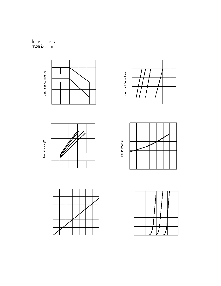
Figure 1. Current Derating Curves
Figure 2. Typical Control Current Requirements
Figure 3. Typical On-Characteristics
Figure 4. Typical On-Resistance
Figure 5. Typical Normalized Off-State Leakage
Figure 6. Input Characteristics (Current Controlled)
PVAZ172N
4
www.irf.com
90%
10%
I
I
LED
D
t
dly
t
on
t
off
Delay Time (microseconds)
50
100
200
500
20
1000
2000
20
10
5
3
toff
tdly
ton
Vds, Drain to Source Voltage (V)
10
0
20
30
40
50
0
450
600
300
150
Figure 7. Typical Delay Times
Figure 9. Typical Output
Capacitance
Figure 8. Delay Time Definitions
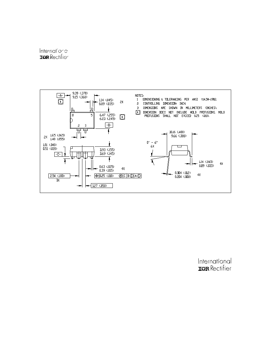
Case Outline
01-2013 00 (MS-001AB)
PVAZ172N
www.irf.com
5
01-2019 00
Case Outline
IR WORLD HEADQUARTERS: 233 Kansas St., El Segundo, California 90245 Tel: (310) 252-7105
IR EUROPEAN REGIONAL CENTRE: 439/445 Godstone Rd., Whyteleafe, Surrey CR3 0BL, United Kingdom
Tel: ++ 44 (0) 20 8645 8000
IR JAPAN: K&H Bldg., 2F, 30-4 Nishi-Ikebukuro 3-Chome, Toshima-Ku, Tokyo, Japan 171-0021 Tel: 8133 983 0086
IR HONG KONG: Unit 308, #F, New East Ocean Centre, No. 9 Science Museum Road, Tsimshatsui East, Kowloon
Hong Kong Tel: (852) 2803-7380
Data and specifications subject to change without notice. 8/5/2000