PD 1.025D
Series PVD33
Microelectronic
Power IC Relay
Single-Pole, 220mA, 0-300V DC
BOSFET
®
Photovoltaic Relay
General Description
The Photovoltaic DC Relay (PVD) is a single-pole, nor-
mally open solid state replacement for electro-me-
chanical relays used for general purpose switching of
analog signals. It utilizes as an output switch a unique
bidirectional (AC or DC) MOSFET power IC termed a
BOSFET. The BOSFET is controlled by a photovoltaic
generator of novel construction, which is energized by
radiation from a dielectrically isolated light emitting di-
ode (LED).
The PVD overcomes the limitations of both conven-
tional and reed electromechanical relays by offering
the solid state advantages of long life, high operating
speed, low pick-up power, bounce-free operation, low
thermal voltages and miniaturization. These advan-
tages allow product improvement and design innova-
tions in many applications such as process control,
multiplexing, telecommunications, automatic test
equipment and data acquisition.
The PVD can switch analog signals from thermocouple
level to 300 volts peak DC. Signal frequencies into the
RF range are easily controlled and switching rates up
to 6kHz are achievable. The extremely small thermally
generated offset voltages allow increased measure-
ment accuracies.
Unique silicon technology developed by International
Rectifier forms the heart of the PVD. The monolithic
BOSFET contains a bidirectional N-channel power
MOSFET output structure. In addition, this power IC
chip has input circuitry for fast turn-off and gate protec-
tion functions. This section of the BOSFET chip utilizes
both bipolar and MOS technology to form NPN transis-
tors, P-channel MOSFETs, resistors, diodes and ca-
pacitors.
The photovoltaic generator similarly utilizes a unique
International Rectifier alloyed multijunction structure.
The excellent current conversion efficiency of this tech-
nique results in the very fast response of the PVD mi-
croelectronic power IC relay.
This advanced semiconductor technology has created
a radically new control device. Designers can now de-
velop switching systems to new standards of electrical
performance and mechanical compactness.
PVD33 Features
BOSFET Power IC
s
s
s
s
s
10
10
Operations
s
s
s
s
s
100µsec Operating Time
s
s
s
s
s
3 milliwatts Pick-Up Power
s
s
s
s
s
1000V/µsec dv/dt
s
s
s
s
s
Bounce-Free
s
s
s
s
s
8-pin DIP Package
s
s
s
s
s
-40°C to 85°C
s
s
s
s
s
UL recognized
s
s
s
s
s
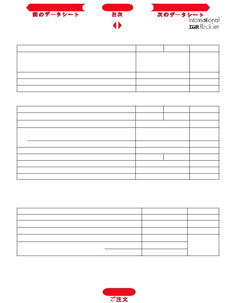
Part Identification
Part Number
Operating
Sensitivity
Off-State
Voltage (DC)
Resistance
PVD2352
200V
10
8
Ohms
5 mA
PVD3354
300V
10
10
Ohms
(BOSFET is a trademark of International Rectifier)
Next Data Sheet
Index
Previous Datasheet
To Order
Series PVD33 BOSFET
®
Photovoltaic Relay
INPUT CHARACTERISTICS
PVD2352
PVD3354
Units
Minimum Control Current
(see figures 1 and 2)
DC
For 160mA Continuous Load Current
2.0
mA@25°C
For 200mA Continuous Load Current
5.0
mA@40°C
For 90mA Continuous Load Current
5.0
mA@85°C
Maximum Control Current for Off-State Resistance at 25°C
10
µA(DC)
Control Current Range (Caution: current limit input LED. See figure 6)
2.0 to 25
mA(DC)
Maximum Reverse Voltage
7.0
V(DC)
Electrical Specifications (-40
°
C
T
A
+85
°
C unless otherwise specified
)
GENERAL CHARACTERISTICS (PVD2352 and PVD3354)
Units
Dielectric Strength: Input-Output
2500
V
RMS
Insulation Resistance: Input-Output @ 90V
DC
10
12
@ 25°C - 50% RH
Maximum Capacitance: Input-Output
1.0
pF
Max. Pin Soldering Temperature
(1.6mm below seating plane, 10 seconds max.)
+260
Ambient Temperature Range:
Operating
-40 to +85
°
C
Storage
-40 to +100
OUTPUT CHARACTERISTICS
PVD2352
PVD3354
Units
Operating Voltage Range
200
300
V
(peak)
Maxiumum Load Current 40°C (see figures 1and 2)
220
mA
(DC)
Response Time @25°C (see figures 7 and 8)
Max. T(on) @ 12mA Control, 50 mA Load, 100 VDC
100
µs
Max. T(off) @ 12mA Control, 50 mA Load, 100 VDC
50
µs
Max. On-state Resistance 25°C
(Pulsed) (fig. 4) 50 mA Load, 5mA Control
6
Min. Off-state Resistance 25°C (see figure 5)
10
8
@ 160VDC
10
10
@ 240VDC
Max. Thermal Offset Voltage @ 5.0mA Control
0.2
µvolts
Min. Off-State dv/dt
1000
V/µs
Output Capacitance (see figure 9)
20
pF @ 50VDC
Next Data Sheet
Index
Previous Datasheet
To Order
Series PVD33 BOSFET
®
Photovoltaic Relay
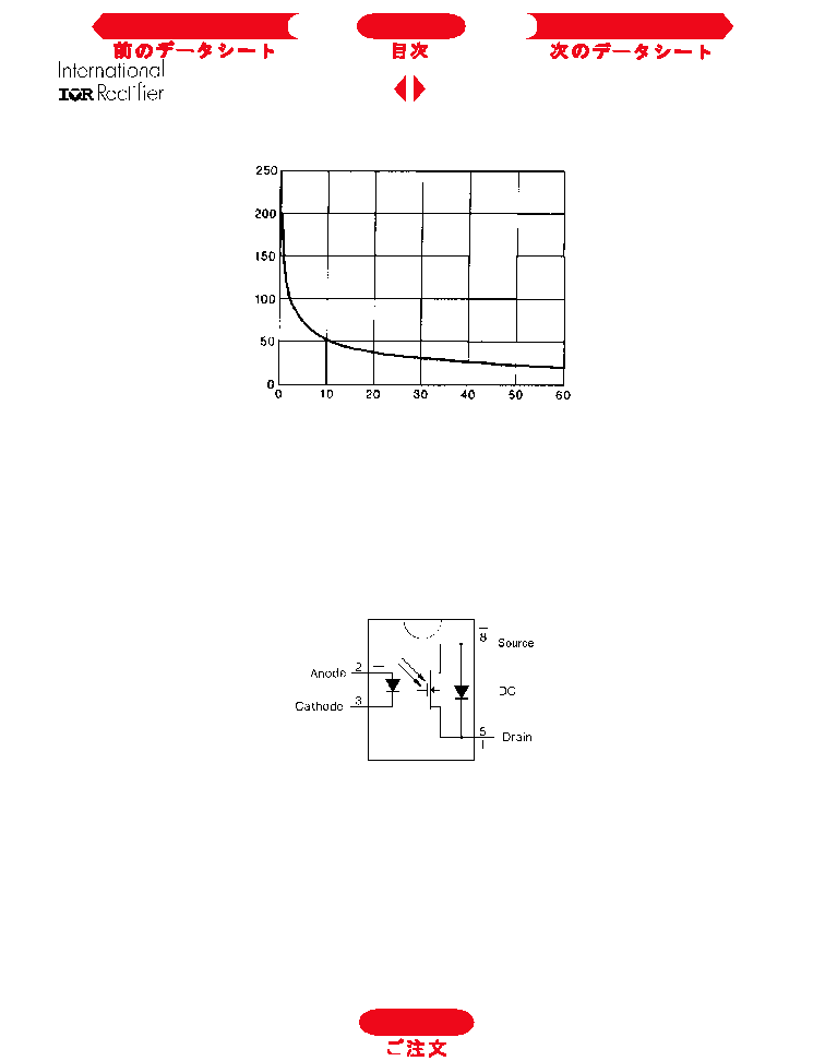
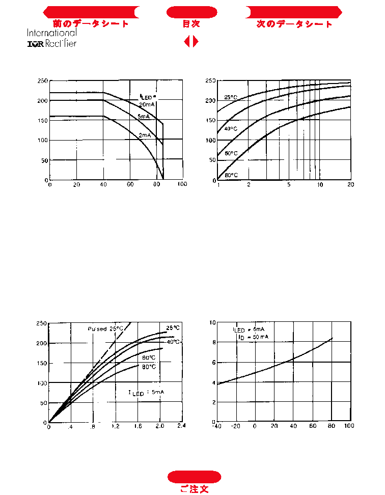
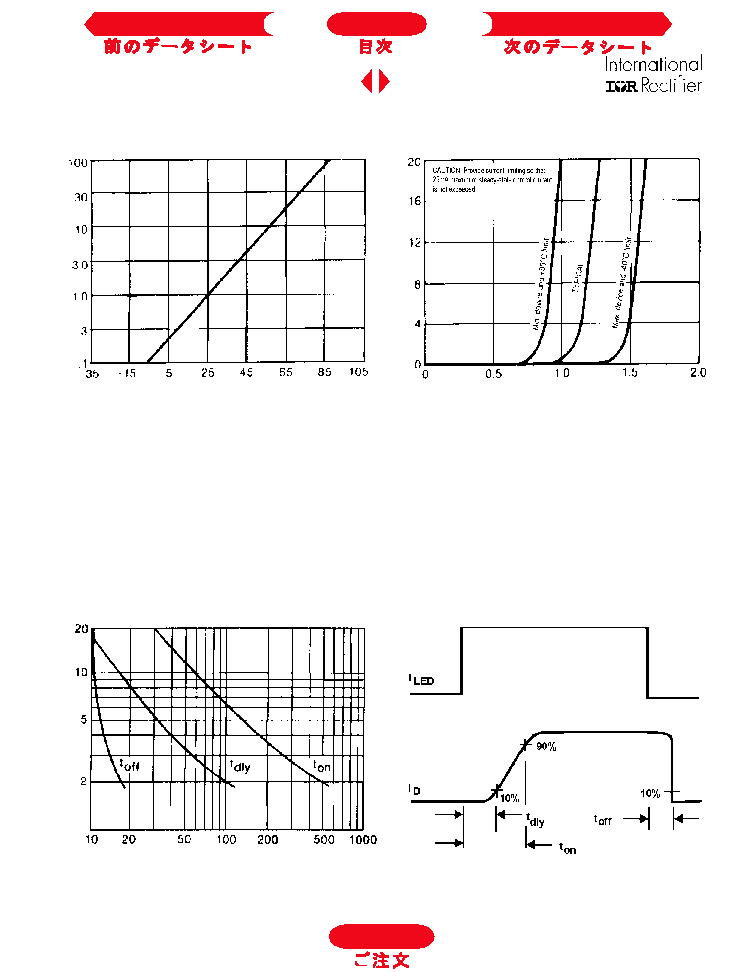
Max. Load Current (mA)
Figure 1. Current Derating Curves
Figure 2. Typical Control Current
Requirements
Figure 3.Typical On Characteristics
Figure 4. Typical On-Resistance
R
DS(on)
(
)
ILED (mA)
Max. Load Current (mA)
Ambient Temperature (°C)
VDS (Volts)
Load Current (mA)
Ambient Temperature (°C)
To Order
Next Data Sheet
Index
Previous Datasheet
Series PVD33 BOSFET
®
Photovoltaic Relay
I D
O
f
f/I
D
Of
f 25°C
Figure 5. Normalized Off-State Leakage
Figure 6. Input Characteristics
(Current Controlled)
Figure 7.Typical Delay Times
Figure 8. Delay Time Definitions
LED Forward Voltage Drop (Volts DC)
Input Current (mA)
Ambient Temperature (°C)
I LED
(mA)
Delay Time (microseconds)
To Order
Next Data Sheet
Index
Previous Datasheet