 | –≠–ª–µ–∫—Ç—Ä–æ–Ω–Ω—ã–π –∫–æ–º–ø–æ–Ω–µ–Ω—Ç: PVG613S | –°–∫–∞—á–∞—Ç—å:  PDF PDF  ZIP ZIP |

Data Sheet No. PD 10058-B
Series PVG613
Microelectronic Power IC
HEXFET
Æ
Power MOSFET Photovoltaic Relay
Single Pole, Normally Open, 0-60V, 1.0A AC/ 2.0 A DC
General Description
The PVG613 Series Photovoltaic Relay is a single-
pole, normally open solid-state relay that can replace
electromechanical relays in many applications. It util-
izes International Rectifier's proprietary HEXFET
power MOSFET as the output switch, driven by an
integrated circuit photovoltaic generator of novel
construction. The output switch is controlled by ra-
diation from a GaAlAs light emitting diode (LED)
which is optically isolated from the photovoltaic
generator.
These units exceed the performance capabilities of
electromechanical relays in operating life, sensitiv-
ity, stable on-resistance, low off-state leakage, minia-
turization, insensitivity to magnetic fields and
ruggedess. The compact PVG613 is particularly suited
for isolated switching of high currents from 12 to 48
Volt AC or DC power sources.
Series PVG613 Relays are packaged in a 6-pin, molded
DIP package with either through-hole or surface mount
(gull-wing) terminals. It is available in standard plastic
shipping tubes or on tape-and-reel. Please refer to Part
Identification information opposite.
Features
!
Bounce-free operation
!
High load current capacity
!
Extremely low off-state leakage
!
Linear AC/DC operation
!
4,000 V
RMS
I/O Isolation
!
Solid-State reliability
!
UL recognized
!
ESD Tolerance:
4000V Human Body Model
500V Machine Model
Applications
!
Industrial Control
!
Computers and Peripheral Devices
!
Audio Equipment
!
Power Supplies and Power Distribution
!
Factory Automation
Part Identification
PVG613
through-hole
PVG613S
surface-mount
PVG613S-T
surface-mount, tape and reel
(HEXFET is the registered trademark for International Rectifier Power MOSFETs)

Series PVG613
2
www.irf.cim
INPUT CHARACTERISTICS
Limits
Units
Minimum Control Current
(see figure 1)
5.0
mA
Maximum Control Current for Off-State Resistance
@ T
A
= +25∞C
0.4
mA
Control Current Range
(Caution: current limit input LED, see figure 6)
5.0 to 25
mA
Maximum Reverse Voltage
7.0
V
OUTPUT CHARACTERISTICS
Limits
Units
Operating Voltage Range
0 to ±60
V
(DC or AC peak)
Maximum Load Current
@ TA = +40∞C, 10mA Control (see figure 1)
A Connection
1.0
A (AC or DC)
B Connection
1.5
A (DC)
C Connection
2.0
A (DC)
Maximum Pulsed Load Current
@ TA
=+25∞C (100 ms @ 10% Duty Cycle)
A Connection
2.4
A (AC or DC)
Maximum On-State Resistance
@T
A
=+25∞C
For 1A pulsed load, 10mA Control (see figure 4)
A Connection
500
m
B Connection
250
m
C Connection
150
m
Maximum Off-State Leakage
@T
A
=+25∞C, ±48V (see figure 5)
10
nA
Maximum Turn-On Time
@T
A
=+25∞C (see figure 7)
For 500mA, 50 V
DC
load, 10mA Control
2.0
ms
Maximum Turn-Off Time
@T
A
=+25∞C (see figure 7)
For 500mA, 50 V
DC
load, 10mA Control
0.5
ms
Maximum Output Capacitance
@ 50V
DC
(see figure 2)
130
pF
Electrical Specifications (-40∞C
T
A
+85∞C unless otherwise specified
)
Connection Diagrams
GENERAL CHARACTERISTICS
Limits
Units
Minimum Dielectric Strength, Input-Output
4000
V
RMS
Minimum Insulation Resistance,
Input-Output, @T
A
=+25∞C, 50%RH, 100V
DC
10
12
Maximum Capacitance, Input-Output
1.0
pF
Maximum Pin Soldering Temperature
(10 seconds maximum)
+260
Ambient Temperature Range:
Operating
-40 to +85
∞C
Storage
-40 to +100
Series PVG613
www.irf.com
3
M
a
.
L
o
a
d Cur
r
e
nt
(
A)
Ambient Temperature (deg. C)
20
40
60
80
100
0
0.25
0.50
0
1.00
1.25
0.75
ILED 10 mA
5 mA
=
'A' Connection
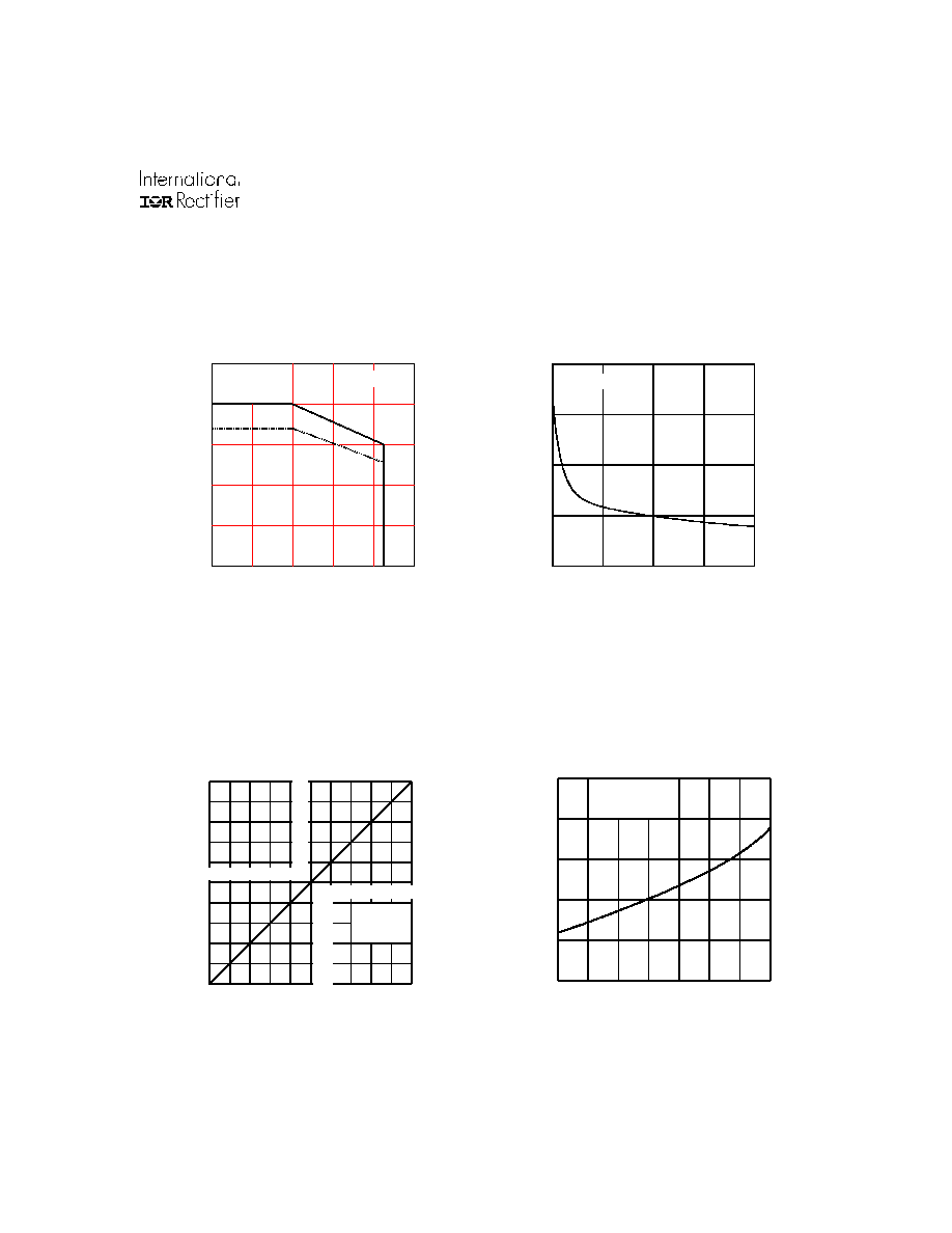
Figure 1. Current Derating Curves*
Figure 2. Typical Output Capacitance
Typic
a
l
C
a
pacit
a
n
c
e
(
pF
)
Vdd, Drain to Drain Voltage (V)
0
15
30
45
60
450
300
150
0
600
'A' Connection
Lo
ad Cur
r
e
nt
(
A)
@25C, pulsed
10 mA Control
-0.1
-0.2
-0.3
-0.4
-0.5
0.50
1.25
1.00
0.25
0.75
-0.25
-1.25
-1.00
-0.75
-0.50
0.5
0.4
0.3
0.2
0.1
Connection 'A' Voltage Drop (Vdd)
R
d
-o
n
(
N
o
r
m
a
li
z
e
d t
o
2
5
deg. C)
Ambient Temperature (deg. C)
2.5
2.0
1.5
1.0
0.5
0
-50
-25
0
25
50
75
100
125
10 mA Control
= 500 mA
D
I
'A' Connection
Figure 3. Linearity Characteristics
Figure 4. Typical Normalized On-Resistance
* Derating of `B' and `C' connection at +85∞C will be 70% of that specified at +40∞C and is linear from +40∞C to +85∞C.

Series PVG613
4
www.irf.cim
LE
D
Cur
r
e
nt
(m
A
)
Delay Time (microseconds)
50
100
200
500
20
1000 2000
20
10
5
3
toff
tdly
ton
90%
10%
I
ILED
D
tdly
ton
toff
Figure 7. Typical Delay Times
Figure 8. Delay Time Definitions
Ambient Temperature (deg. C)
-35
-15
5
25
45
65
85
10 5
100
30
10
3.0
1.0
0.3
0.1
I D-
O
F
F
2
5
d
e
g
. C
/
I
D-O
F
F
In
p
u
t
C
u
rren
t
(
mA
)
LED Forward Voltage Drop (Volts DC)
16
20
12
8
4
0
0.5
1.0
1.5
2.0
0
not eceeded
T
YP
I
C
A
L
CAUTION: provide current limiting
so that 25 mA maimum steady-
state control current rating is
M
i
n
. d
e
v
ic
e
a
nd
+8
5
d
e
g
.
C
lim
i
t
M
a
. d
e
v
i
c
e
a
nd
-
40
d
e
g
.
C
l
im
i
t
Figure 5. Typical Normalized Off-State Leakage
Figure 6. Input Characteristics (Current Controlled)

Series PVG613
www.irf.com
5
IR WORLD HEADQUARTERS: 233 Kansas St., El Segundo, California 90245 Tel: (310) 252-7105
Data and specifications subject to change without notice. 2/18/2003
01-2008 01
Case Outlines
01-2009 01