 | –≠–ª–µ–∫—Ç—Ä–æ–Ω–Ω—ã–π –∫–æ–º–ø–æ–Ω–µ–Ω—Ç: PVI5013R | –°–∫–∞—á–∞—Ç—å:  PDF PDF  ZIP ZIP |
Data Sheet No. 1.1041
Series PVI5013R
Solid-State
Opto-Isolated MOSFET Gate Driver
Dual-Channel
5V, 1.0
µ
A
General Description
The PVI5013R Photovoltaic Isolator is a dual-
channel, opto-isolated driver capable of directly
driving gates of power MOSFETs or IGBTs. It
utilizes a monolithic integrated circuit photovoltaic
generator of novel construction as its output. The
output is controlled by radiation from a GaAlAs
light emitting diode (LED) which is optically
isolated from the photovoltaic generator.
The PVI5013R is ideally suited for applications
requiring high-current and/or high voltage
switching with optical isolation between the low-
level driving circuitry and high-energy or high-
voltage load circuits. It can be used for directly
driving gates of power MOSFETs. The dual-
channel configuration allows its outputs to drive
independent discrete power MOSFETs, or be
connected in parallel or in series to provide
higher-current drive for power MOSFETs or
higher-voltage drive for IGBTs. PVI5013R
employs a fast turn-off circuitry.
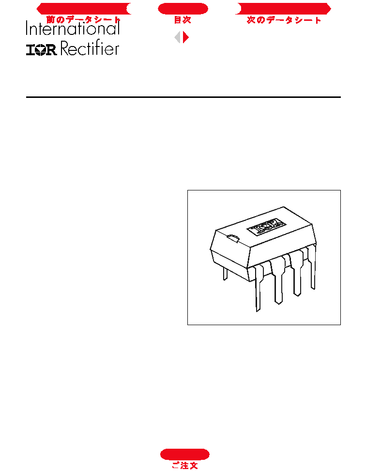
PVI5013R Photovoltaic Isolators are packaged
in an 8-pin, molded DIP package with either thru-
PVI5013R Features
Monolithic construction
s
s
s
s
s
3,750 V
RMS
I/O isolation
s
s
s
s
s
1,200 V
DC
output-to-output isolation
s
s
s
s
s
Dual-Channel application flexibility
s
s
s
s
s
Solid-State reliability
s
s
s
s
s
UL and CSA certifications pending
s
s
s
s
s
Part Identification
PVI5013R
thru-hole
PVI5013RS
SMT
PVI5013RS-T
SMT, T&R
PHOTOVOLTAIC ISOLATOR
hole or "gull-wing" terminals. It is available in
standard plastic shipping tubes or on tape-and-
reel. Refer to Part Identification information.
Applications
Telecommunications
s
s
s
s
s
Load Distribution
s
s
s
s
s
Industrial Controls
s
s
s
s
s
Instrumentation and Measurement
s
s
s
s
s
Next Data Sheet
Index
Previous Datasheet
To Order

PVI5013R
Electrical Specifications (-40∞C
T
A
+85∞C unless otherwise specified
)
INPUT CHARACTERISTICS
Limits
Units
Min. Input Current (See Fig.1)
5.0
mA
Input Current Range (See Fig. 1)
3.0 to 25
mA
Max. Continuous Input Current @ T
A
=+25∞C
40
mA
LED Forward Voltage Drop @ 5mA, T
A
=+25∞C (See Fig. 3)
1.4
V
Max. Reverse Voltage
7.0
V
Max. Reverse Current @ -7V
DC
, T
A
=+25∞C
10
µA
OUTPUT CHARACTERISTICS
Limits
Units
Min. Forward Voltage
8.0
V
DC
Max. Reverse Current
10
µA
DC
COUPLED CHARACTERISTICS
Limits
Units
Min. Output Voltage @ I
LED
= 5mA, R
L
= 10M
3
V
@ T
A
=0∞C to +70∞C (See Fig. 1 & 2)
Max. Output Voltage @ I
LED
= 5mA, R
L
= 10M
8
V
@ T
A
=0∞C to +70∞C (See Fig. 1 & 2)
Max. Voltage Differential Between Outputs
1.0
V
@ I
LED
= 5mA, R
L
= 10M
Typical Output Short-Circuit Current
1.0
µA
@ I
LED
= 5mA, @ T
A
=+25∞C (See Fig. 1 & 2)
Max. Turn-On Time @ I
LED
= 5mA, C
LOAD
= 200pF (See Fig. 4)
5
ms
Max. Turn-Off Time @ I
LED
= 5mA, C
LOAD
= 200pF (See Fig. 4)
0.25
ms
Off-State Clamping Resistance: minimum
100
maximum
3300
GENERAL CHARACTERISTICS
Limits
Units
Min. Dielectric Strength, Input-Output
3750
V
RMS
Min. Dielectric Strength, Output-to-Output
1200
V
DC
Min. Insulation Resistance, Input-to-Output
@TA=+25∞C, 50%RH, 100VDC
Max. Capacitance, Input-Output
5.0
pF
Max. Pin Soldering Temperature (10 seconds max.)
+260
∞C
Ambient Temperature Range: Operating
-40 to +85
∞C
Storage
-40 to +125
∞C
Connection Diagram
10
12
5 (-)
6 (+)
7 (-)
8 (+)
1
2
3
4
Next Data Sheet
Index
Previous Datasheet
To Order

Figure 1. Typical Output Characteristics
Figure 2. Typical Variation of Output
Figure 3. Input Characteristics (Current Controlled)
Figure 4. Typical Response Time
PVI5013R
Load Capacitance (pF)
R
esponse T
i
m
e
(
m
i
c
r
o
seconds)
100
200
300
400
500
500
100
50
1000
5000
ILED=5mA
Toff
Ton
60
-40
0
20
40
80
100
-20
Ambient Temperature (deg. C)
N
o
r
m
al
i
z
ed O
u
t
put
0.5
0.6
0.7
0.8
0.9
1.0
1.1
1.2
ILED=5mA
Short-Circuit Current
Output Voltage
Input Current (mA)
O
u
t
put
V
o
l
t
age (
V
D
C
)
10
20
0
30
40
9.0
0
12
10
8
6
4
2
0
1.5
3.0
4.5
6.0
7.5
Rl=10MOhm
Open Circuit Voltage
I
nput
C
u
r
r
ent
(
m
A
)
LED Forward Voltage Drop (Volts DC)
16
20
12
8
4
0
0.5
1.0
1.5
2.0
0
CAUTION: provide current limiting
so that 25 mA maximum steady-
state control current rating is
not exceeded
Min. device and +85 deg. C limit
TYPICAL
Max. device and -40 deg. C limit
Short-Circuit Current
Output Short-Circuit Current (uA)
To Order
Next Data Sheet
Index
Previous Datasheet

1. DIMENSIONING AND TOLERANCING PER ANSI Y14.5M-1982
2. CONTROLLING DIMENSION: INCH
4 DIMENSION DOES NOT INCLUDE MOLD PROTRUSIONS. MOLD
PROTRUSIONS SHALL NOT EXCEED 0.25 (.010).
Mechanical Specifications
(Dimensions in millimeters (inches))
WORLD HEADQUARTERS: 233 Kansas St., El Segundo, California 90245, Tel: (310) 322 3331
EUROPEAN HEADQUARTERS: Hurst Green, Oxted, Surrey RH8 9BB, UK Tel: (44) 0883 713215
IR CANADA: 7321 Victoria Park Ave., Suite 201, Markham, Ontario L3R 3L1, Tel: (905) 475 1897
IR GERMANY: Saalburgstrasse 157, 61350 Bad Homburg Tel: 6172 37066
IR ITALY: Via Liguria 49, 10071 Borgaro, Torino Tel: (39) 1145 10111
IR FAR EAST: K&H Bldg., 2F, 3-30-4 Nishi-Ikeburo 3-Chome, Toshima-Ki, Tokyo 171 Tel: (03)3983 0641
IR SOUTHEAST ASIA: 315 Outram Road, #10-02 Tan Boon Liat Building, Singapore 0316 Tel: 65 221 8371
http://www/irf.com/
Data and specifications subject to change without notice. 6/96
PVI5013R
To Order
Next Data Sheet
Index
Previous Datasheet