 | ÐлекÑÑоннÑй компоненÑ: PVN012S-T | СкаÑаÑÑ:  PDF PDF  ZIP ZIP |
PVN012_E.p65
Data Sheet No. PD 10034-E
Series PVN012
Microelectronic Power IC
HEX.ET
®
Power MOS.ET Photovoltaic Relay
Single Pole, Normally Open, 0-20V, 2.5A AC/ 4.5A DC
General Description
The PVN012 Series Photovoltaic Relay at 100
milliohms features the lowest possible on-state
resistance in a miniature package -- lower than a
comparable reed relay.
The PVN012 is a single-pole, normally open solid-
state relay. It utilizes a GenerationV HEXFET output
switch, driven by an integrated circuit photovoltaic
generator of novel construction. The output switch is
controlled by radiation from a GaAlAs light emitting
diode (LED) which is optically isolated from the
photovoltaic generator.
These units exceed the performance capabilities of
electromechanical relays in life, sensitivity, stable on-
resistance, miniaturization, magnetic insensitivity and
ruggedness. They are ideally suited for switching
high currents or low level signals without distortion
or injection of electrical noise.
Series PVN012 Relays are packaged in a
6-lead molded DIP package with either through-hole
or surface mount (gull-wing) terminals. They are avail-
able in standard plastic shipping tubes or on tape-
and-reel. Please refer to part identification information
opposite.
Applications
§
Portable Electronics
§
Programmable Logic Controllers
§
Computers and Peripheral Devices
§
Audio Equipment
§
Power Supplies and Power Distribution
§
Instrumentation
Part Identification
PVN012
through-hole
PVN012S
surface-mount
PVN012S-T
surface-mount, tape and reel
(HEXFET is the registered trademark for International Rectifier Power MOSFETs)
Features
§
100m
On-Resistance
§
GenV HEXFET output
§
Bounce-free operation
§
2.5 - 4.5 Amp capacity
§
Linear AC/DC operation
§
4,000 V
RMS
I/O isolation
§
Solid-State reliability
§
UL recognized
§
ESD Tolerance:
4000V Human Body Model
500V Machine Model
www.irf.com
1
Series PVN012
2
www.irf.com
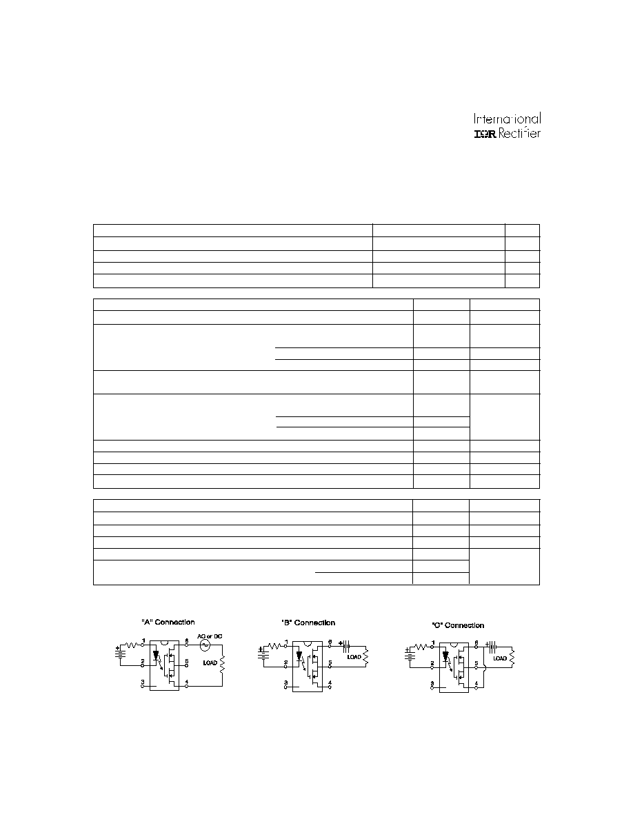
Connection Diagrams
GENERAL CHARACTERISTICS
Limits
Units
Minimum Dielectric Strength,
Input-Output
4000
VRMS
Minimum Insulation Resistance,
Input-Output, @T
A
=+25°C, 50%RH, 100V
DC
10
12
Maximum Capacitance,
Input-Output
1.0
pF
Maximum Pin Soldering Temperature
(10 seconds maximum)
+260
Ambient Temperature Range:
Operating
-40 to +85
°C
Storage
-40 to +100
OUTPUT CHARACTERISTICS
Limits
Units
Operating Voltage Range
0 to ±20
V(DC or AC peak)
Maximum Continuous Load Current
@ T
A
=+40°C, 5mA Control (see figure 1)
A Connection
2.5
A (DC or AC)
B Connection
3.0
A (DC)
C Connection
4.5
A (DC)
Maximum Pulsed Load Current
@T
A
=+25°C, (100 ms @ 10% duty cycle)
A Connection
6.0
A (DC or AC)
Maximum On-State Resistance
@T
A
=+25°C, for 1A pulsed load, 5mA Control (see figure 4)
A Connection
100
B Connection
65
m
C Connection
40
Minimum Off-State Resistance
@ T
A
=+25°C, ±16V
DC
0.16 x 10
8
Maximum Turn-On Time
@T
A
=+25°C (see figure 7), for 1A, 20 V
DC
load, 5mA Control
5.0
ms
Maximum Turn-Off Time
@T
A
=+25°C (see figure 7), for 1A, 20 V
DC
load, 5mA Control
0.5
ms
Maximum Output Capacitance
@ 20V
DC
(see figure 2)
300
pF
INPUT CHARACTERISTICS
Limits
Units
Minimum Control Current
(see figure 1)
3.0
mA
Maximum Control Current for Off-State Resistance
@ T
A
= +25°C
0.4
mA
Control Current Range
(Caution: current limit input LED, see figure 6)
3.0 to 25
mA
Maximum Reverse Voltage
7.0
V
Electrical Specifications (-40°C
T
A
+85°C unless otherwise specified
)
Series PVN012
www.irf.com
3
Vdd, Drain to Drain Voltage (V)
0
5
10
15
20
800
600
400
200
0
"A" Connection
1000
Ambient Temperature (deg. C)
20
40
60
80
100
0
1.0
2.0
0
3.0
ILED 5 mA
3 mA
=
"A" Connection
0.5
1.5
2.5
ILED =
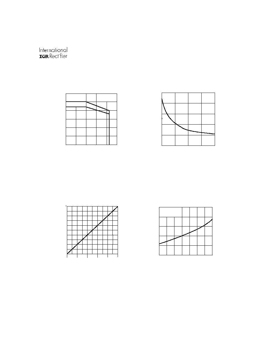
Figure 1. Current Derating Curves*
Figure 2. Typical Output Capacitance
T
ypical Capacitance (pF)
Max. Load Current (A)
0.05
0.10
0.15
0.20
0.25
-0.05
-0.10
-0.15
-0.20
-0.25
-0.5
-1.0
-1.5
-2.0
0.5
1.0
1.5
2.5
Connection "A" Voltage Drop (Vdd)
-2.5
2.0
0
0
5 mA Control @ 25°C, pulsed
Ambient Temperature (deg. C)
2.5
2.0
1.5
1.0
0.5
0
-50
-25
0
25
50
75
100
125
5 mA Control
"A" Connection
ID = 1 A
Load Current (A)
Rd-on (Nor
malized to 25° C)
Figure 3. Linearity Characteristics
Figure 4. Typical Normalized On-Resistance
* Derating of `B' and `C' connection at +85°C will be 70% of that specified at +40°C and is linear from +40°C to +85°C.
Series PVN012
4
www.irf.com
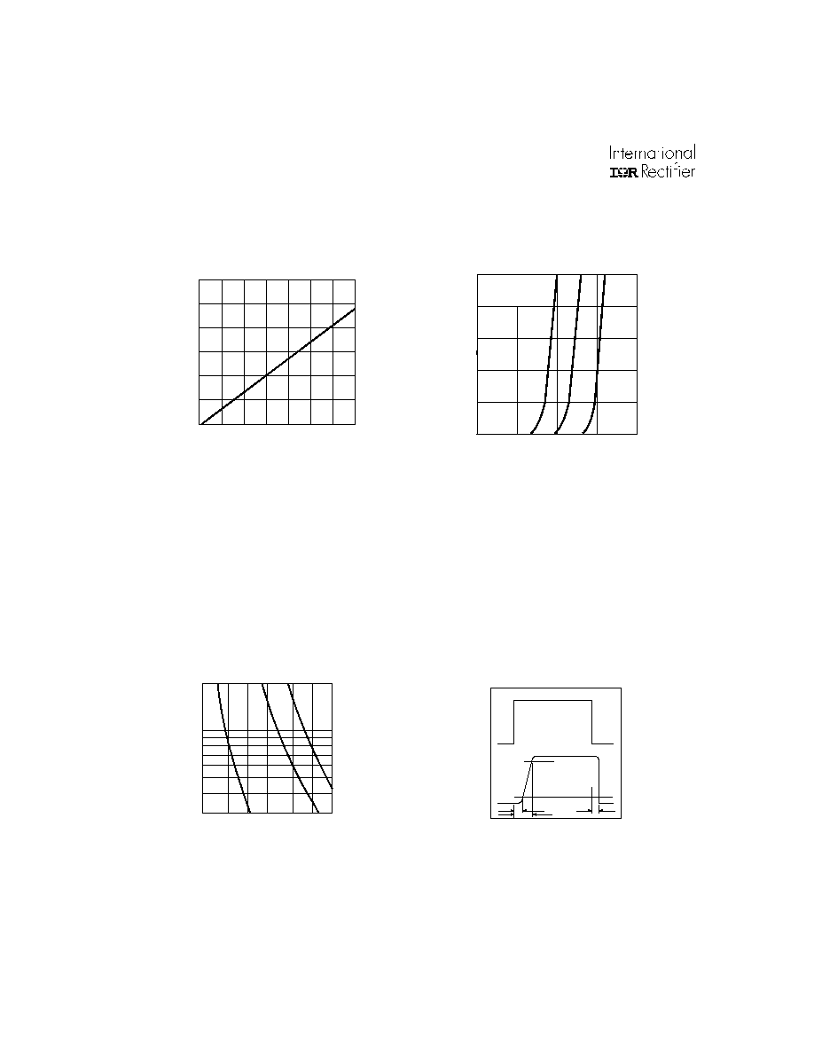
90%
10%
I
ILED
D
tdly
ton
toff
Figure 7. Typical Delay Times
Figure 8. Delay Time Definitions
20
10
5
3
toff
tdly
ton
0.1
0.2
0.5
1.0
2.0
5.0
0.05
LED Current (mA)
Delay Time (milliseconds)
Ambient Temperature (deg. C)
-35
-15
5
25
45
65
85
105
100
30
10
3.0
1.0
0.3
0.1
I
D-OFF
/ I
D-OFF
25°C
Input Current (mA)
16
20
12
8
4
0
TYPICAL
Min. device and +85 deg. C limit
Max. device and -40 deg. C limit
CAUTION: provide current
limiting so that 25mA
maximum steady state
control current rating is
not exceeded.
0
0 . 5
1 . 0
1 . 5
2 . 0
LED Forward Voltage Drop (Volts DC)
Figure 5. Typical Normalized Off-State
Figure 6. Input Characteristics
(Current Controlled)
Leakage
Series PVN012
www.irf.com
5
IR WORLD HEADQUARTERS: 233 Kansas St., El Segundo, California 90245 Tel: (310) 252-7105
Data and specifications subject to change without notice. 7/5/2002
01-2008 01
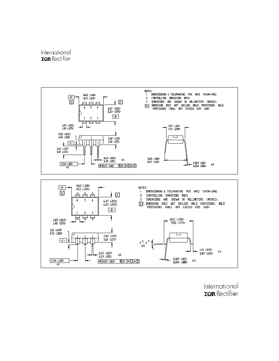
Case Outlines
01-2009 01