/home/web/doc/html/irf/194470

Data Sheet No. PD10045C
PVO402AP
Microelectronic Power IC
HEXFET
®
Power MOSFET Relay
Single Pole, Normally Open + Ring Detector
0-400V, 150mA AC/DC
(HEXFET is the registered trademark for International Rectifier Power MOSFETs)
General Description
The PVO402AP Photovoltaic Relay is a single pole,
normally open solid-state relay plus ring detector. By
integrating these two functions in one package it can
replace two discrete components, i.e., a relay and an
AC-input opto-coupler. The relay portion of PVO402AP
utilizes International Rectifier's HEXFET power
MOSFET as the output switch, driven by an integrated
circuit photovoltaic generator of novel construction. The
output switch is controlled by radiation from a GaAlAs
light emitting diode (LED) which is optically isolated from
the photovoltaic generator. The ring detector portion of
PVO402AP has two LEDs in inverse parallel connec-
tion as the input sensing element and a silicon NPN
photo-transistor as the output switch.
PVO402AP is ideally suited for PCMCIA fax/modem
cards. Its extremely low profile allows it to be used in
Type II cards whose outer shells are only 5mm thick.
PVO402AP Relays are packaged in an 8-pin, molded
`Thin-Pak' DIP package with `gull-wing' surface mount
terminals. It is available in plastic shipping tubes or on
tape-and-reel. Please refer to Part Identification (oppo-
site) for details.
Applications
§
On/Off Hook switch
§
Dial pulsing
§
Ringer injection
§
Ring detection
§
Loop current detection
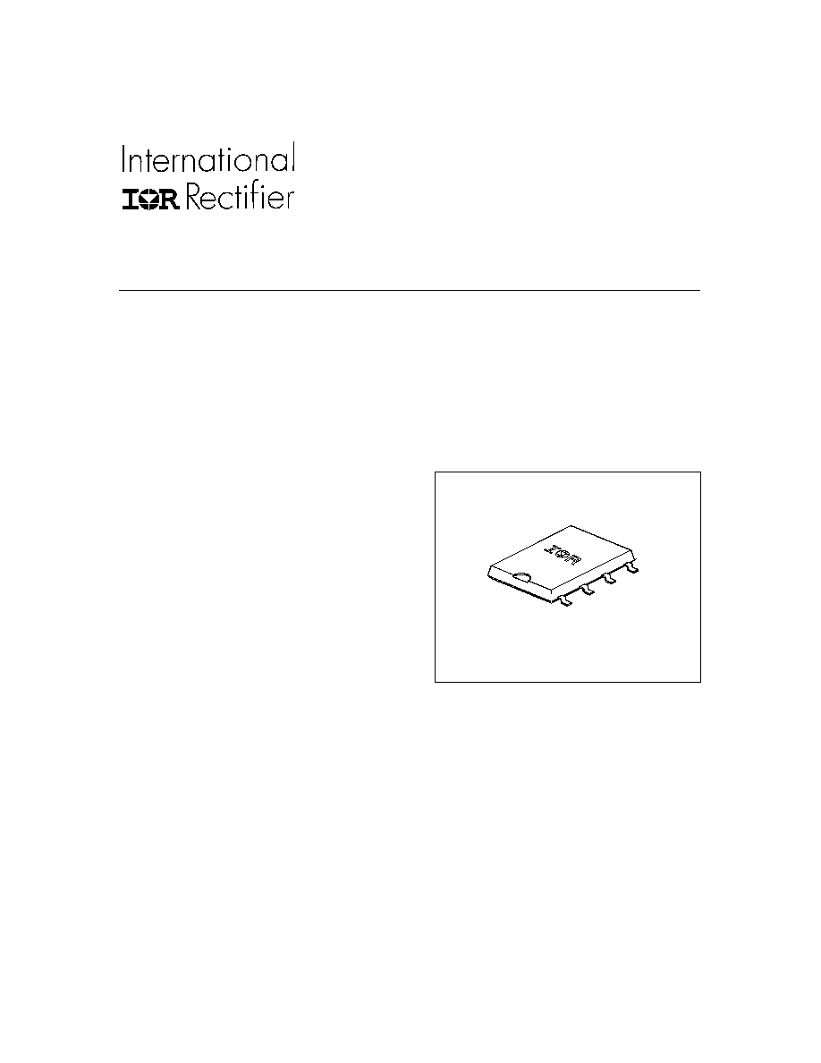
PVO402AP `Thin-Pak'
Features
§
HEXFET Power MOSFET output
§
Bounce-free operation
§
3,750 V
RMS
I/O Isolation
§
Linear AC/DC operation
§
Solid-State Reliability
§
BABT certified
Part Identification
PVO402AP
SMT, plastic shipping tube
PVO402AP-T
SMT, tape and reel

PVO402AP
2
www.irf.com
GENERAL CHARACTERISTICS
Limits
Units
Min. Dielectric Strength, Input-Output
3750
V
RMS
Min. Dielectric Strength, Relay-Detector
1000
V
DC
Min. Insulation Resistance, Input-Output
@T
A
=+25
°
C, 50%RH, 100V
DC
10
12
Max. Capacitance, Input-Output
3.0
pF
Max. Pin Soldering Temperature (10 seconds max.)
+260
Ambient Temperature Range: Operating
-40 to +85
°
C
Storage
-40 to +100
Electrical Specifications (-40
°
C
T
A
+85
°
C unless otherwise specified
)
INPUT CHARACTERISTICS
Limits
Units
Min. Control Current @ I
C
= 2mA, V
CE
= 0.5V
5.0
mA
Max. Control Current for Off-State Leakage I
C
=1µA, V
CE
=5V @T
A
=+25
°
C
5
µA
Control Current Range (Caution: current limit input LED, see Fig.6)
5.0 to 25
mA
DETECTOR
INPUT CHARACTERISTICS
Limits
Units
Min. Control Current (See Fig.1)
5.0
mA
Max. Control Current for Off-State Resistance @TA=+25
°
C
0.4
mA
Control Current Range (Caution: current limit input LED, see Fig.6)
5.0 to 25
mA
Max. Reverse Voltage
7.0
V
RELAY
OUTPUT CHARACTERISTICS
Limits
Units
Operating Voltage Range
0 to ±400
V
(DC or AC peak)
Max. Load Current @ T
A
=+40
°
C
5mA Control (See Fig.1)
150
mA
Max. On-State Resistance @T
A
=+25
°
C
For 50mA Pulsed Load, 5mA Control (See Fig.4)
22
Max. Off-State Leakage @T
A
=+25°C, ±400V (See Fig.5)
1.0
µA
Max. Turn-On Time @T
A
=+25
°
C (See Fig. 7)
For 50mA, 100 V
DC
Load, 5mA Control
1.0
ms
Max. Turn-Off Time @T
A
=+25
°
C (See Fig. 7)
For 50mA, 100 V
DC
Load, 5mA Control
0.5
ms
Max. Output Capacitance @ 50V
DC
12
pF
OUTPUT CHARACTERISTICS
Limits
Units
Min. Collector-Emitter Breakdown Voltage @ I
C
= 10µA
20
V
DC
Min.Current Transfer Ratio @ I
LED
= 6mA, V
CE
= 5V (see Fig. 9)
33
%
Max. Saturation Voltage @ I
LED
= 16mA, I
C
= 2mA
0.5
V
Max. Leakage Current @ I
LED
=0mA, V
CE
= 5V
500
nA
Max. Power Dissipation @T
A
=+25
°
C (derate linearly 2.0mW/
°
C)
150
mW
COMBINED

PVO402AP
www.irf.com
3
Vdd, Drain to Drain Voltage (V)
0
10
20
30
40
50
200
150
100
50
0
Relay
Max. Load Current (mA)
T
ypical Capacitance (pF)
Connection Diagram
1
2
8
7
6
3
4
5
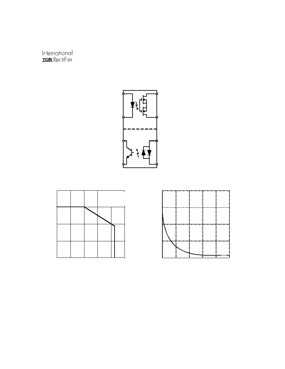
Figure 1. Current Derating Curve
Figure 2. Typical Output Capacitance
20
40
60
80
100
0
0
200
Relay
5 mA
=
LED
I
150
100
50
Ambient Temperature (deg. C)
Relay
I
LED
= 5mA

PVO402AP
4
www.irf.com
Load Current (mA)
Rd-on (Normalized to 25 deg. C)
Ambient Temperature (deg. C)
-35
-15
5
25
45
65
85
105
100
30
10
3.0
1.0
0.3
0.1
Relay
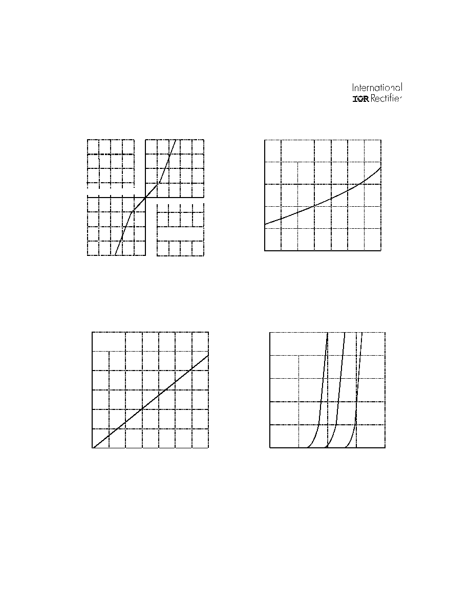
Figure 3. Linearity Characteristics
Figure 4. Typical Normalized On-Resistance
Ambient Temperature (deg. C)
2.5
2.0
1.5
1.0
0.5
0
-50
-25
0
25
50
75
100
125
5 mA Control
I D = 10 mA
Relay
2 . 0
3 . 0
4 . 0
5 . 0
1 . 0
-1.0
-2.0
-3.0
-4.0
-5.0
- 5 0
- 1 0 0
- 1 5 0
- 2 0 0
5 0
1 0 0
1 5 0
2 0 0
5 m A C o n t r o l
@ 25
°
C, pulsed
Relay's Output Voltage Drop (Vdd)
1 6
2 0
1 2
8
4
0
0 . 5
1 . 0
1 . 5
2 . 0
0
LED Forward Voltage Drop (Volts DC)
Figure 5. Typical Normalized Off-State
Leakage
Figure 6. Input Characteristics
(Current Controlled)
Input Current (mA)
I
D-OFF
/ I
D-OFF
25
°
deg. C
CAUTION: Provide current
limiting so that 25mA max.
steady-state control current
rating is not exceeded.
Relay and
Detector
Min.
de
vice and +85
°C limit
TYPICAL
Max.
de
vice and -40
°C limit

PVO402AP
www.irf.com
5
LED Current (mA)
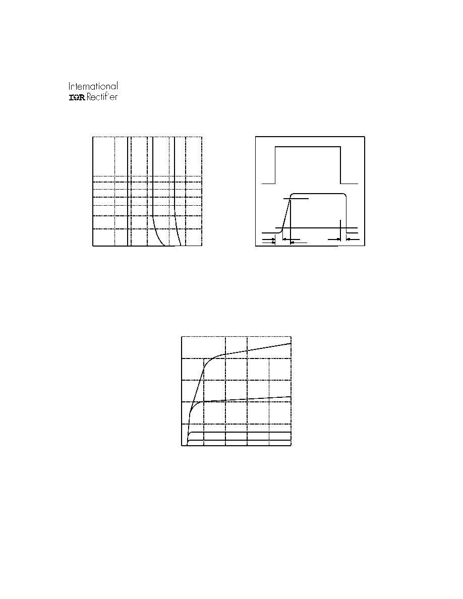
Figure 7. Typical Delay Times
Figure 8. Delay Time Definitions
Figure 9.Typical Transfer Characteristics
Delay Time (microseconds)
50
100
200
500
20
1000 2000
20
10
5
3
toff
tdly
ton
Relay
90%
10%
I
I LED
D
tdly
ton
t off
Collector-Emitter Voltage (V)
Detector
2
4
6
8
10
0
10
20
30
0
40
50
1 mA
2 mA
5 mA
10 mA
ILED =
Collector Current (mA)
