Data Sheet No. PD10042-D
Series PVT322
Microelectronic Power IC
HEXFET
®
Power MOSFET Photovoltaic Relay
Dual Pole, Normally Open
0-250V, 170mA AC/DC
(HEXFET is the registered trademark for International Rectifier Power MOSFETs)
General Description
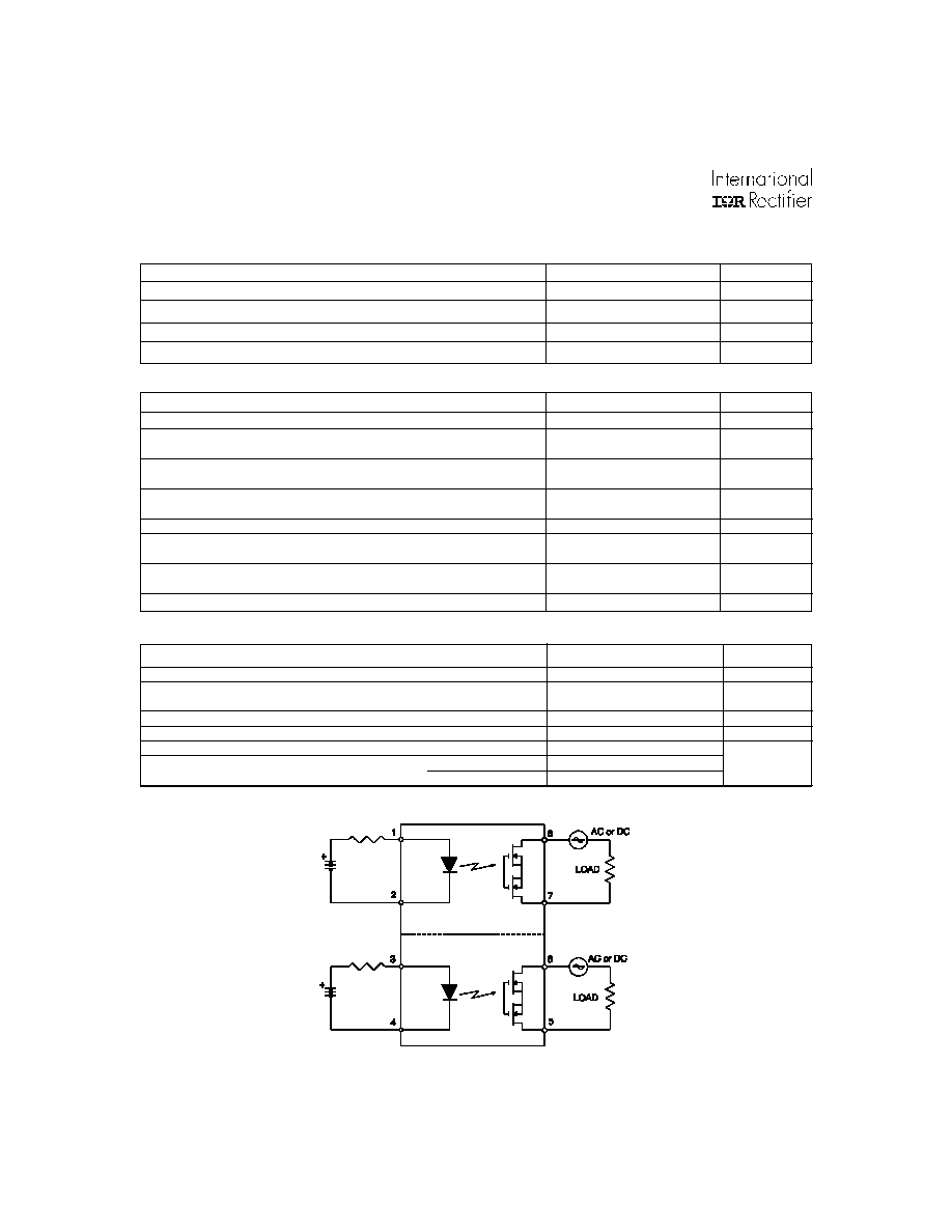
The PVT322 Series Photovoltaic Relay is a dual-
pole, normally open solid-state relay that can re-
place electromechanical relays in many applications.
It utilizes International Rectifier's HEXFET power
MOSFET as the output switch, driven by an inte-
grated circuit photovoltaic generator of novel con-
struction. The output switch is controlled by radia-
tion from a GaAlAs light emitting diode (LED) which
is optically isolated from the photovoltaic generator.
Series PVT322 Relays are packaged in an 8-pin,
molded DIP package with either through-hole or
surface mount (gull-wing) terminals. It is available
in standard plastic shipping tubes or on tape-and-
reel. Please refer to Part Identification information
opposite.
Applications
"
On/Off Hook switch
"
Tip and Ring Line switching
"
General switching
Part Identification
PVT322
thru-hole
PVT322S
SMT
PVT322S-T
SMT, T&R
Features
"
HEXFET Power MOSFET output
"
Bounce-free operation
"
4,000 V
RMS
I/O isolation
"
Linear AC/DC operation
"
Solid-State Reliability
"
UL recognized and BABT certified
Series PVT322
2
www.irf.com
Electrical Specifications (-40°C
T
A
+85°C unless otherwise specified
)
INPUT CHARACTERISTICS
Limits
Units
Minimum Control Current
(See figure1)
2.0
mA
Maximum Control Current for Off-State Resistance
@TA=+25°C
0.4
mA
Control Current Range
(Caution: current limit input LED, see figure 5)
2.0 to 25
mA
Maximum Reverse Voltage
7.0
V
Connection Diagram
OUTPUT CHARACTERISTICS
Limits
Units
Operating Voltage Range
0 to ±250
V
(DC or AC peak)
Maximum Load Current
@ T
A
=+40°C
5mA Control (See figure 1) (single and dual channel operation)
170
mA
Maximum Peak Load Current
(10ms maximum duration)
(single and dual channel operation)
500
mA
Maximum On-State Resistance
@T
A
=+25°C
For 50mA Pulsed load, 5mA Control (see figure 3)
10
Maximum Off-State Leakage
@T
A
=+25°C, ±250V (see figure 4)
1.0
µA
Maximum Turn-On Time
@T
A
=+25°C (see figure 6)
3.0
ms
For 50mA, 100 V
DC
load, 5mA Control
Maximum Turn-Off Time
@T
A
=+25°C (see figure 6)
0.5
ms
For 50mA, 100 V
DC
load, 5mA Control
Maximum Output Capacitance
@ 50V
DC
50
pF
GENERAL CHARACTERISTICS
Limits
Units
Minimum Dielectric Strength, Input-Output
4000
V
RMS
Minimum Dielectric Strength, Pole-to-Pole
1000
V
DC
Minimum Insulation Resistance,
Input-Output, @T
A
=+25°C, 50%RH, 100V
DC
10
12
Maximum Capacitance, Input-Output
1.0
pF
Maximum Pin Soldering Temperature
(10 seconds maximum)
+260
Ambient Temperature Range:
Operating
-40 to +85
°C
Storage
-40 to +100
Series PVT322
www.irf.com
3
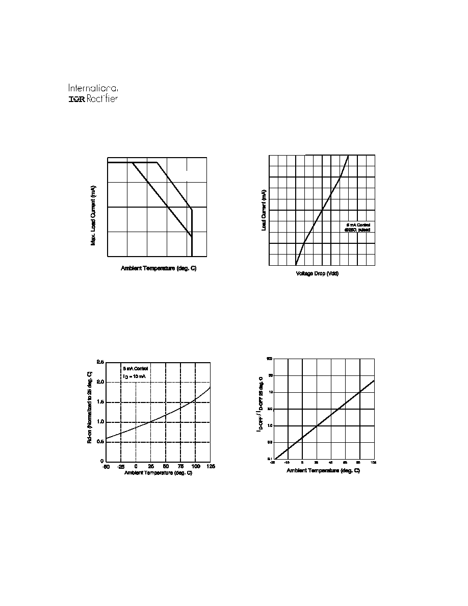
Figure 3. Typical Normalized On-Resistance
0.5
1.0
1.5 2.0 2.5
-0.5
-1.0
-1.5
-2.0
-2.5
-50
-100
-150
-200
50
100
150
200
250
-250
3.0
-3.0
Figure 2. Linearity Characteristics
20
40
60
80
100
0
0
100
200
150
50
Figure 1. Typical Current Derating Curve
Figure 4. Typical Normalized Off-State Leakage
2 mA
ILED = 5 mA
Series PVT322
4
www.irf.com
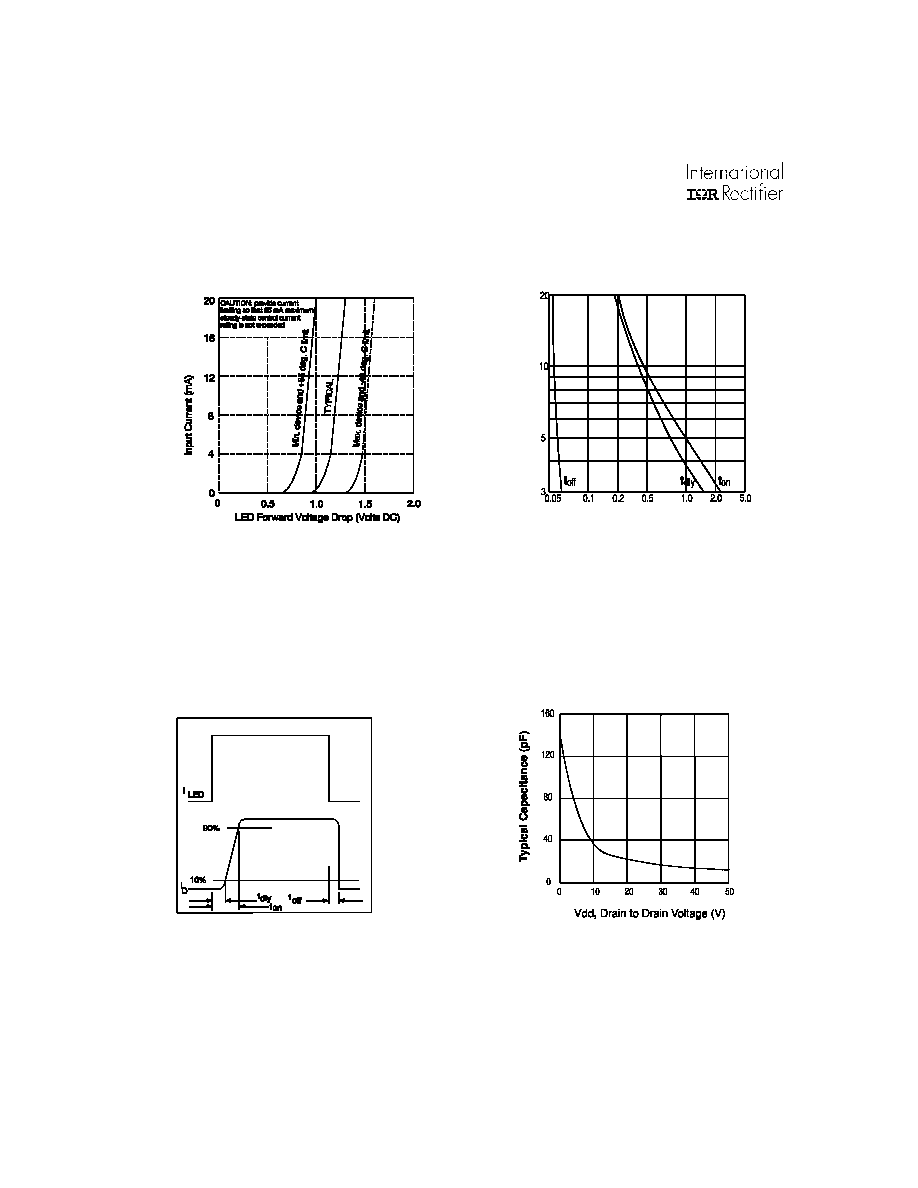
Figure 7. Delay Time Definitions
Figure 8. Typical Output Capacitance
Figure 5. Input Characteristics (Current Controlled)
Figure 6. Typical Delay Times
LED Current (mA)
Delay Time (milliseconds)
Series PVT322
www.irf.com
5
IR WORLD HEADQUARTERS: 233 Kansas St., El Segundo, California 90245 Tel: (310) 252-7105
Data and specifications subject to change without notice. 5/19/2003
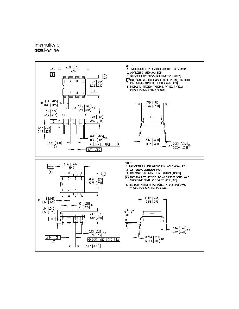
Case Outlines
01-2030 01
01-2031 01