PVT412A_e.p65
Data Sheet No. PD10060-E
Series PVT412A
Microelectronic Power IC
HEXFET
®
Power MOSFET Photovoltaic Relay
Single Pole, Normally Open,
0-400V, 240mA AC / 360mA DC
General Description
The PVT412A Series Photovoltaic Relay is a single-
pole, normally open solid-state relay that can replace
electromechanical relays in many applications. It util-
izes International Rectifier's proprietary HEXFET power
MOSFET as the output switch, driven by an integrated
circuit photovoltaic generator of novel construction. The
output switch is controlled by radiation from a GaAlAs
light emitting diode (LED) which is optically isolated from
the photovoltaic generator.
These SSRs are specifically designed for industrial
control and peripheral telecom applications.
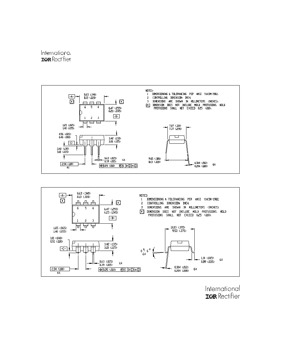
Series PVT412A Relays are packaged in a 6-lead
molded DIP package with either through-hole or sur-
face mount (`gull-wing') terminals. It is available in stan-
dard plastic shipping tubes or on tape-and-reel. Please
refer to part identification information
.
Applications
!
Control of AC power line
(up to 240 VAC) industrial loads
!
Control of DC industrial loads
up to +/-300 VDC
!
On/Off hook switch
!
Dial-pulse generation
Part Identification
PVT412A
through-hole
PVT412AS
surface-mount
PVT412AS-T
surface-mount, Tape and Reel
(HEXFET is the registered trademark for International Rectifier Power MOSFETs)
Features
!
HEXFET Power MOSFET output
!
Bounce-free operation
!
4,000 V
RMS
I/O isolation
!
Very low on-resistance (R
DD-ON
)
!
Linear AC/DC operation
!
Solid-State Reliability
!
UL recognized
!
ESD Tolerance:
4000V Human Body Model
500V Machine Model
www.irf.com
1
Series PVT412A
2
www.irf.com
OUTPUT CHARACTERISTICS
Limits
Units
Operating Voltage Range
0 to ±400
V peak
Maximum Load Current
@ T
A
=+40°C 5mA Control (see figure 1)
A Connection
240
mA
B Connection
260
mA
C Connection
360
mA
Maximum On-State Resistance
@T
A
=+25°C
100mA Pulsed Load, 5mA Control (see figures 2 & 3)
A Connection
6
B Connection
3
C Connection
2
Max. pulsed Load Current
@T
A
=+25°C, ±400V, 5mA Control (10mS @ 10% duty cycle)
750
mA
Maximum Off-State Leakage
@T
A
=+25°C, ±400V
1.0
µA
Maximum Turn-On Time
@T
A
=+25°C (see figures 6 & 7)
For 50mA, 100 V
DC
load, 5mA Control (5mS pulse width @ 50% duty cycle)
3.0
ms
Maximum Turn-Off Time
@T
A
=+25°C (see figures 6 & 7)
For 50mA, 100 V
DC
load, 5mA Control (5mS pulse width @ 50% duty cycle)
0.5
ms
Maximum Output Capacitance
@ 50V
DC
, f=1MHz (Cout, see figure 8)
40.0
pF
INPUT CHARACTERISTICS
Limits
Units
Minimum Control Current
(see figure 1)
3.0
mA
Maximum Control Current for Off-State Resistance
0.4
mA
Control Current Range
(Caution: current limit input LED, see figure 5)
3.0 to 25
mA
Maximum Reverse Voltage
7.0
V
Electrical Specifications
0-400V, 240ma,AC (TA = +25°C
)
unless otherwise specified
)
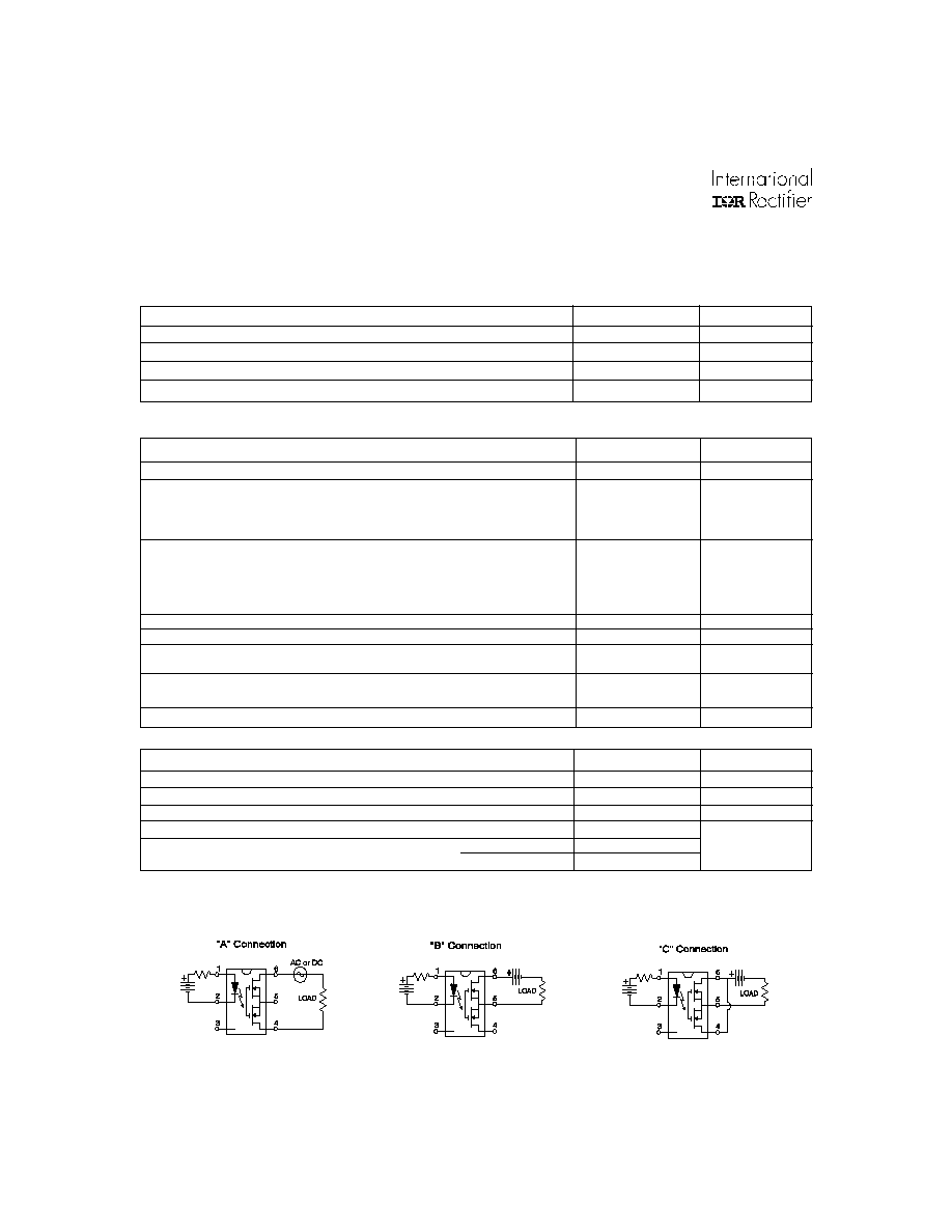
Connection Diagrams
GENERAL CHARACTERISTICS
Limits
Units
Minimum Dielectric Strength, Input-Output
4000
V
RMS
Minimum Insulation Resistance, Input-Output
10
12
Maximum Capacitance, Input-Output Vd=0V, f=1MHz
1.0
pF
Maximum Pin Soldering Temperature (10 seconds maximum)
+260
Ambient Temperature Range:
Operating
-40 to +85
°C
Storage
-40 to +100
Series PVT412A
www.irf.com
3
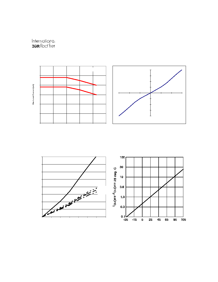
0
50
100
150
200
250
300
0
20
40
60
80
100
Figure 2. Typical On Characteristics
Ambient Temperature (C)
Figure 1. Current Derating Curves
V
DD
(Volts) Ambient
Figure 3. Typical On-Characteristics
-800
-600
-400
-200
0
200
400
600
800
-3.0
-2.0
-1.0
0.0
1.0
2.0
3.0
Voltage Drop (V
DD
)
Load Current (mA
)
I LED = 5mA
20mS Pulsed, 25C
0
100
200
300
400
500
600
700
800
0.0
0.5
1.0
1.5
2.0
2.5
3.0
3.5
Load Current (mA)
I
LE D
= 5mA
20m S - P ulse d , 25ºC
25-40ºC
60ºC
85ºC
"A" Connection
"A" Connection
Ambient Temperature (
o
C)
Figure 4. Typical Normalized Off-State Leakage
"A" Connection
I
LED
= 5mA
I
LED
= 3mA
Series PVT412A
4
www.irf.com
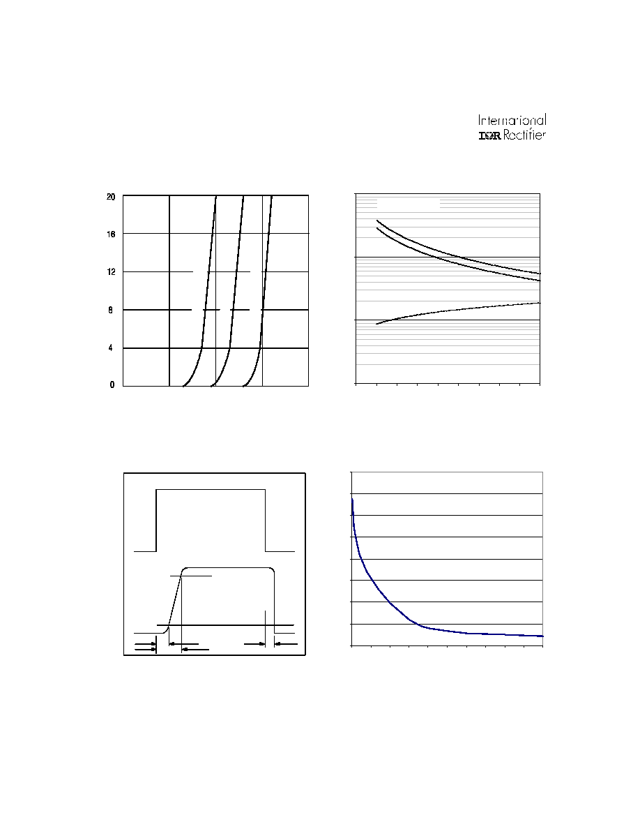
Figure 6. Typical Delay Times
Figure 8. Typical Output Capacitance
0.01
0.10
1.00
10.00
1
2
3
4
5
6
7
8
9
10
I LED (mA)
Delay Time (mS
)
Ton
Tdly
Figure 5. Input Characteristics (Current Controlled)
TYPICAL
min. device & +85°C limit
max. device & -45°C limit
0
0.5 1.0 1.5 2.0
LED Forward Voltage Drop (Volts DC)
Input Current (mA)
Toff
"A" Connection
I
D
10%
tdly
ton
toff
I
LED
90%
Figure 7. Delay Time Definitions
0
50
100
150
200
250
300
350
400
0
5
10
15
20
25
30
35
40
45
50
V
DD
Drain to Drain Voltage
Typical Capacitance (pF)
"A" Connection
Series PVT412A
www.irf.com
5
IR WORLD HEADQUARTERS: 233 Kansas St., El Segundo, California 90245 Tel: (310) 252-7105
Data and specifications subject to change without notice. 6/28/2003
01-2009 01
01-2008 01
Case Outlines