Data Sheet No. PD 10037-C
Series PVT422
Microelectronic Power IC
HEXFET
®
Power MOSFET Photovoltaic Relay
Dual Pole, Normally Open
0-400V, 120mA AC/DC
General Description
The PVT422 Series Photovoltaic Relay is a dual-
pole, normally open solid-state relay that can replace
electromechanical relays in many applications. It util-
izes International Rectifier's HEXFET power MOSFET
as the output switch, driven by an integrated circuit
photovoltaic generator of novel construction. The
output switch is controlled by radiation from a GaAlAs
light emitting diode (LED) which is optically isolated
from the photovoltaic generator.
Series PVT422 Relays are packaged in an 8-pin,
molded DIP package with either through-hole or
surface mount (gull-wing) terminals. It is available in
standard plastic shipping tubes or on tape-and-reel.
Please refer to Part Identification information oppo-
site.
(HEXFET is the registered trademark for International Rectifier Power MOSFETs)
Applications
!
On/Off Hook switch
!
Dial-Out relay
!
Ring injection relay
!
General switching
Part Identification
PVT422
through-hole
PVT422S
surface-mount
PVT422S-T
surface-mount, Tape and Reel
Features
!
HEXFET Power MOSFET output
!
Bounce-free operation
!
4,000 V
RMS
I/O isolation
!
Linear AC/DC operation
!
Solid-State Reliability
!
UL recognized and BABT certified
www.irf.com
1
Series PVT422
2
www.irf.com
Electrical Specifications (-40°C
T
A
+85°C unless otherwise specified
)
INPUT CHARACTERISTICS
Limits
Units
Minimum Control Current
(See figure1)
2.0
mA
Maximum Control Current for Off-State Resistance
@TA=+25°C
0.4
mA
Control Current Range
(Caution: current limit input LED, see figure 5)
2.0 to 25
mA
Maximum Reverse Voltage
7.0
V
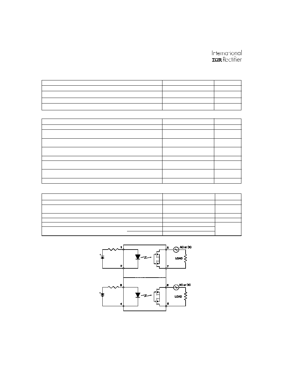
Connection
Diagram
OUTPUT CHARACTERISTICS
Limits
Units
Operating Voltage Range
0 to ±400
V
(DC or AC peak)
Maximum Load Current
@ T
A
=+40°C
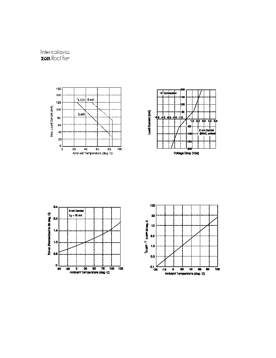
5mA Control (See figure 1) (single and dual channel operation)
120
mA
Maximum Peak Load Current
(10ms maximum duration)
(single and dual channel operation)
350
mA
Maximum On-State Resistance
@T
A
=+25°C
For 50mA Pulsed load, 5mA Control (see figure3)
35
Maximum Off-State Leakage
@T
A
=+25°C, ±320V (see figure 4)
1.0
µA
Maximum Turn-On Time
@T
A
=+25°C (see figure 6)
2.0
ms
For 50mA, 100 V
DC
load, 5mA Control
Maximum Turn-Off Time
@T
A
=+25°C (see figure 6)
2.0
ms
For 50mA, 100 V
DC
load, 5mA Control
Maximum Output Capacitance
@ 50V
DC
12
pF
GENERAL CHARACTERISTICS
Limits
Units
Minimum Dielectric Strength, Input-Output
4000
V
RMS
Minimum Dielectric Strength, Pole-to-Pole
1000
V
DC
Minimum Insulation Resistance,
Input-Output, @T
A
=+25°C, 50%RH, 100V
DC
10
12
Maximum Capacitance, Input-Output
1.0
pF
Maximum Pin Soldering Temperature
(10 seconds maximum)
+260
Ambient Temperature Range:
Operating
-40 to +85
°C
Storage
-40 to +100
Series PVT422
www.irf.com
3
Figure 1. Typical Current Derating Curve
Figure 2. Linearity Characteristics
Figure 3. Typical Normalized On-Resistance
Figure 4. Typical Normalized Off-State Leakage
Series PVT422
4
www.irf.com
Figure 7. Delay Time Definitions
Figure 8. Typical Output Capacitance
Figure 5. Input Characteristics (Current Controlled)
Figure 6. Typical Delay Times
Series PVT422
www.irf.com
5
IR WORLD HEADQUARTERS: 233 Kansas St., El Segundo, California 90245 Tel: (310) 252-7105
Data and specifications subject to change without notice. 5/19/2003
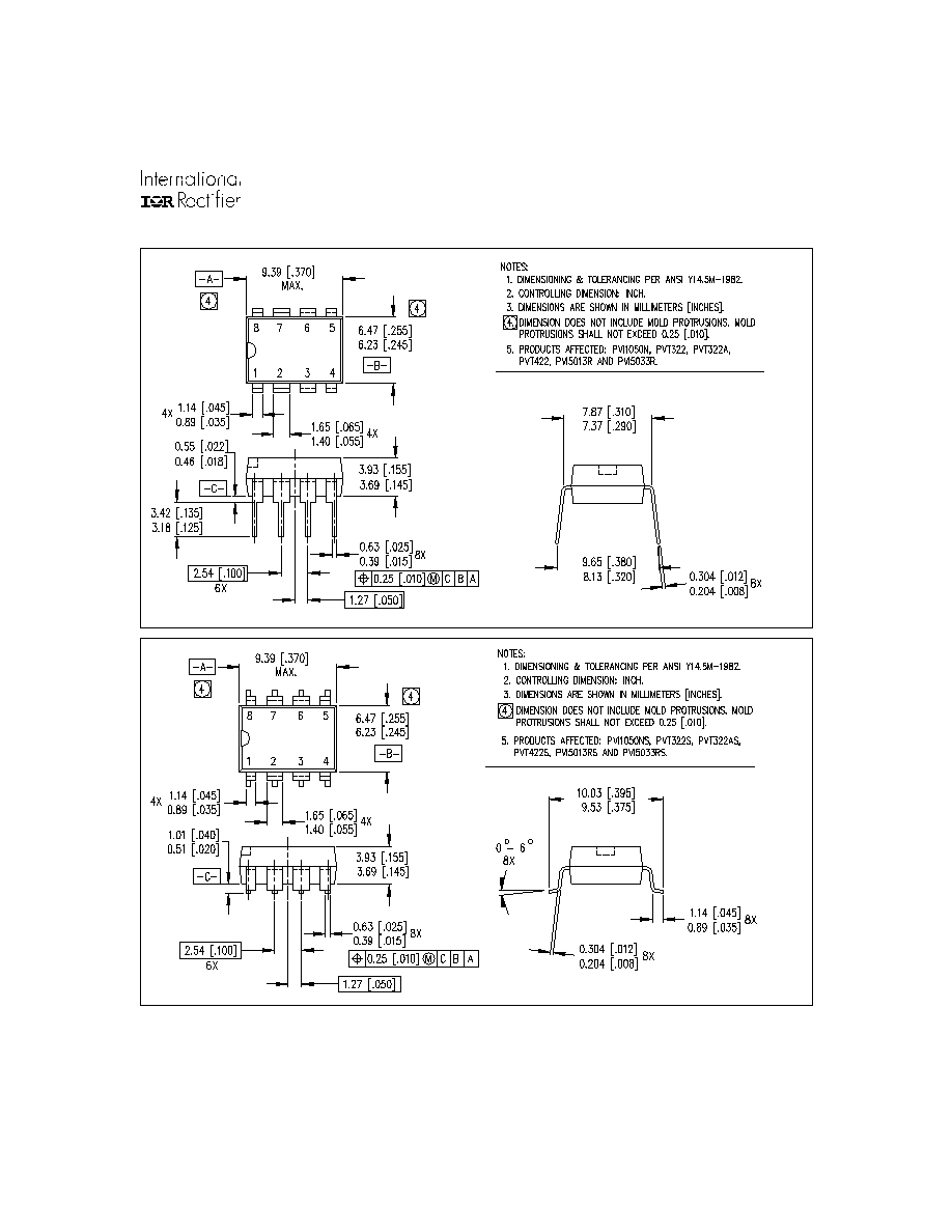
Case Outlines
01-2030 01
01-2031 01