Data Sheet No. PD 10063
Series PVY117
Microelectronic Power IC
HEXFET
®
Power MOSFET Photovoltaic Relay
Single-Pole, Normally-Open, 0-40V AC/DC, 470mA
General Description
The PVY117 Series Photovoltaic Relay is a single-
pole, normally-open solid-state relay that can replace
dry and Mercury-wetted reed relays in many appli-
cations. It utilizes International Rectifier's proprietary
HEXFET power MOSFET as the output switch,
driven by an integrated circuit photovoltaic generator
of novel construction. The output switch is controlled
by radiation from a GaAlAs light emitting diode (LED),
which is optically isolated from the photovoltaic
generator.
The PVY117 is ideally suited for use as matrix relay
in low voltage ATE applications and general
instrumentation applications involving high frequency
test signals. This can be accomplished thanks to the
extremely low Figure Of Merit (FOM = Coff * Ron),
which is the product of the relay's off-state output
capacitance and on-state resistance.
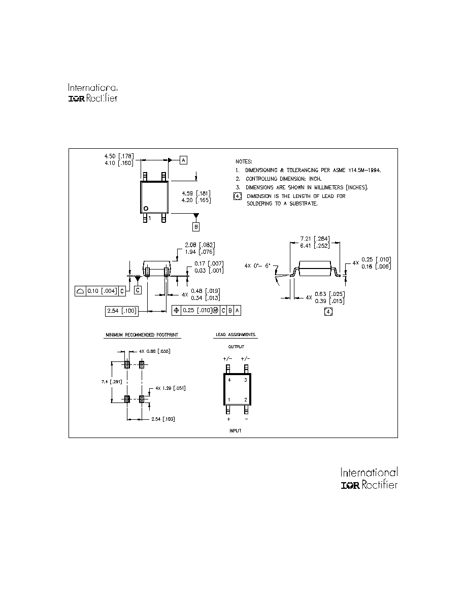
The PVY117 is packaged in a 4-pin, molded small
outline package (SOP-4) with surface mount (gull
wing) terminals. It is available in plastic shipping
tubes or on tape-and-reel. Please refer to Part
Identification information.
Applications
Automated Test Equipment
Instrumentation
Data Acquisition
(HEXFET is the registered trademark for International Rectifier's power MOSFETs)
Part Identification
PVY117
surface-mount
PVY117-T
surface-mount, tape-and-reel
Features
Low signal distortion at high frequencies
Low Coff * Ron Figure Of Merit
High off-state resistance
1,500 V
RMS
I/O isolation
Long operational life
Solid-State Reliability
ESD Tolerance 2000V Human Body Model
Series PVY117
2
www.irf.com
Electrical Specifications
(-40°C
T
A
+85°C unless otherwise specified
)
INPUT CHARACTERISTICS
Units
Min
Typ
Max
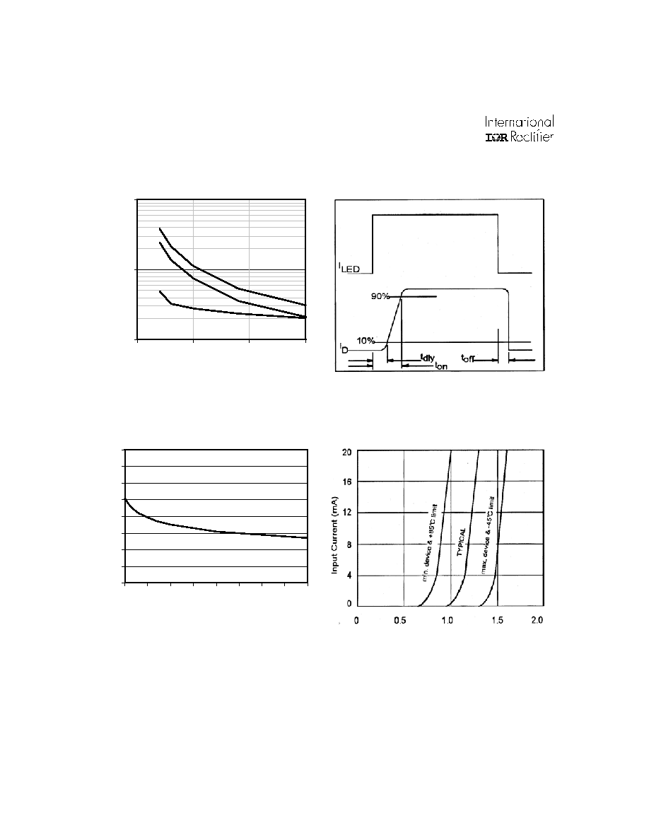
Minimum control current (see Figure 1)
mA
2.0
--
--
Control current for off-state resistance @T
A
= +25°C
mA
--
--
0.2
Control current range (caution: current limit input LED, see Figure 8)
mA
2.0
--
20.0
Reverse voltage
V
--
--
7.0
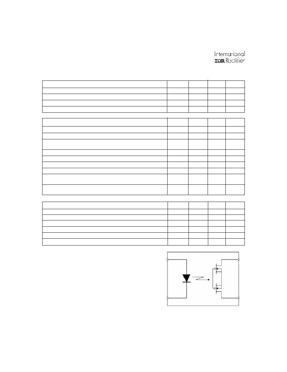
Connection Diagram
GENERAL CHARACTERISTICS
Units
Min
Typ
Max
Dielectric strength, Input to Output
V
RMS
1500
--
--
Insulation Resistance, Input to Output
10
12
--
--
C
I-O
(Input to Output Capacitance), Vd = 0V, f = 1MHz
pF
--
0.8
--
Max. pin soldering temperature (10 seconds max.)
o
C
--
--
+260
Ambient temperature range:
Operating
o
C
-40
--
+85
Storage
o
C
-40
--
+100
OUTPUT CHARACTERISTICS
Units
Min
Typ
Max
Operating voltage range
V peak
--
--
40
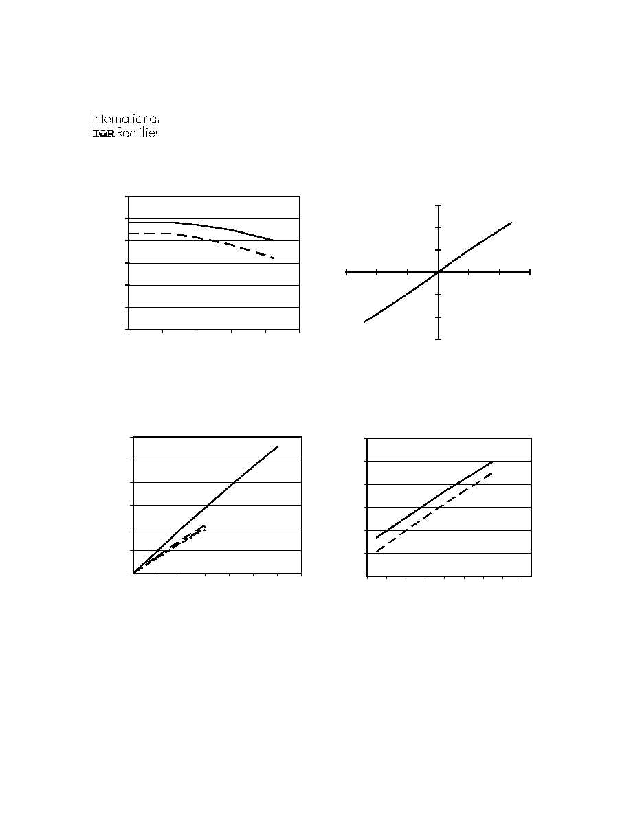
Continuous load current @ 40°C, 5mA control (see Figure 1)
mA
--
--
470
Pulsed load current @ 25°C, 5mA control (see Figures 2 and 3)
mA
--
--
850
10ms on, 10% duty cycle
Off-state leakage @ 40V, 25°C, (see Figure 4)
nA
--
0.05
1.0
On-state resistance @ 5mA control, I
L
=100mA (see Figures 2 and 3)
--
0.74
0.95
Output capacitance Vd=0V, f=1MHz
(Cout, see Figure 7)
pF
--
10.1
14.5
C * R (Cout x RDDon)
pF *
--
7.5
--
Turn-on time, 5mA control, 100
, 20V (Ton, see Figure 5)
µ
S
--
110
200
1ms on, 50% duty cycle
Turn-off time, 5mA control, 100
, 20V (Toff, see Figure 5)
µ
S
--
30
100
1ms on, 50% duty cycle
International Rectifier does not recommend the use
of this product in aerospace, avionics, military or life
support applications. Users of this International Rec-
tifier product in such applications assume all risks
of such use and indemnify International Rectifier
against all damages resulting from such use.
1
2
3
4
Series PVY117
www.irf.com
5
IR WORLD HEADQUARTERS: 233 Kansas Street, El Segundo, California 90245 Tel: (310) 252-7105
This product has been designed and qualified for the Industrial Market
Data and specifications subject to change without notice. 11/6/2004
01-2027 01
Case Outlines - 4 Lead SOP