Äîêóìåíòàöèÿ è îïèñàíèÿ www.docs.chipfind.ru
SCHOTTKY DIE 105 x 125 mils
SC105.....5. Series
www.irf.com
1
Bulletin I0503J 12/99
NOTE:
10 mils die thickness is available on specific request only.
Contact factory for information.
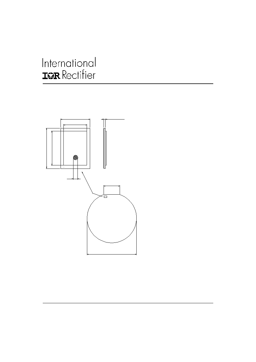
40 (1.57)
Ø 125 (4.92)
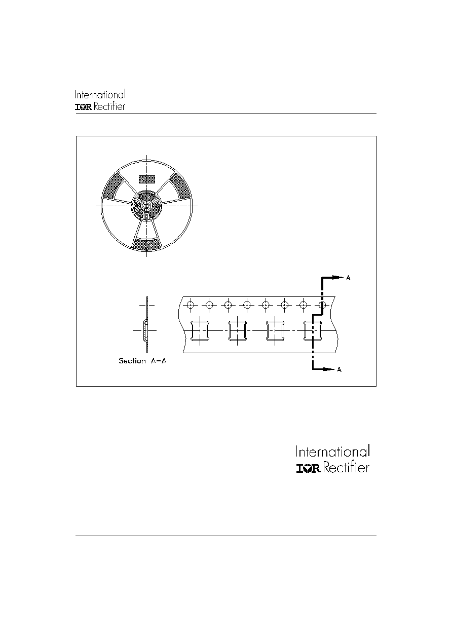
NOTES:
1. ALL DIMENSIONS ARE SHOWN IN MILLIMETERS (INCHES).
2. CONTROLLING DIMENSION: (INCH).
3. DIMENSIONS AND TOLERANCES:
a = 3.18 + 0, - 0.05
(0.125 + 0, - 0.002)
b = 2.67 + 0, - 0.05
(0.105 + 0, - 0.002)
c = 3.02 + 0, - 0.003
(0.119 + 0, - 0.0001)
d = 2.51 + 0, - 0.003
(0.099 + 0, - 0.0001)
Ø = 0.7 ± 0.1
(0.03 ± 0.004)
4. LETTER DESIGNATION:
A = Anode (Top Metal)
C = Cathode (Back Metal)
D = Reject Ink Dot (only on non-conforming dies)
5. SAWING:
Recommended Blade
SEMITEC S1025 QS00 Blade
a
d
Ø
0.35 ± 0.01
C
A
D
c
b
(0.14 ± 0.0004)
Wafer flat alligned with
side b of the die
NOT TO SCALE
SC105.....5. Series
2
Bulletin I0503J 12/99
www.irf.com
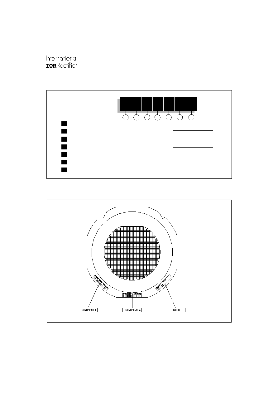
SC105xxxxx5
B
Inked Probed Unsawn Wafer (Wafer in Box)
1150
SC105xxxxx5
R
Probed Die in Tape & Reel
3000
SC105xxxxx5
P
Probed Die in Waffle Pack
1150
SC105xxxxx5
F
Inked Probed Sawn Wafer on Film
1150
Device
T
J
Max.
V
R
Typ. I
R
@ 25°C
Typ. I
R
@ 125°C
Max. V
F
@ I
F
Package
#
(°C)
(V)
(µA)
(mA)
(V)
Style
SC105
R
015x5x
125
15
3000
n.a. contact factory
SC105
S
020x5x
125
20
n.a. contact factory
SC105
S
030x5x
150
30
220
100
0.49 @ 15A
TO-220
SC105
S
045x5x
150
45
150
75
0.54 @ 15A
TO-247
SC105
S
060x5x
150
60
110
60
0.60 @ 15A
TO-247
SC105
H
045x5x
175
45
35
10
0.62 @ 15A
TO-220
SC105
H
100x5x
175
100
12
7
0.86 @ 15A
TO-247
SC105
H
150x5x
175
150
15
7
1.00 @ 15A
TO-220
Electrical Characteristics
Device
Metal Thickness
Metal Thickness
#
Front Metal
Back Metal
SC105xxxx
A
5x
Bondable
--
Al/Si 30 kÅ
--
Cr 1 kÅ
Ni 4 kÅ
Ag 6 kÅ
SC105xxxx
S
5x
Solderable
Ti 2 kÅ
Ni 6 kÅ
Ag 35 kÅ
Cr 1 kÅ
Ni 4 kÅ
Ag 6 kÅ
Mechanical Data
Device
Description
Minimum Order Quantity
#
Wafer in Sale Package
Packaging
Recommended Storage Environment: Store in original container, in dessicated nitrogen, with no contamination.
Shelf life for parts stored in above condition is 2 years.
If the storage is done in normal atmosphere shelf life is reduced to six months.
SC105.....5. Series
3
Bulletin I0503J 12/99
www.irf.com
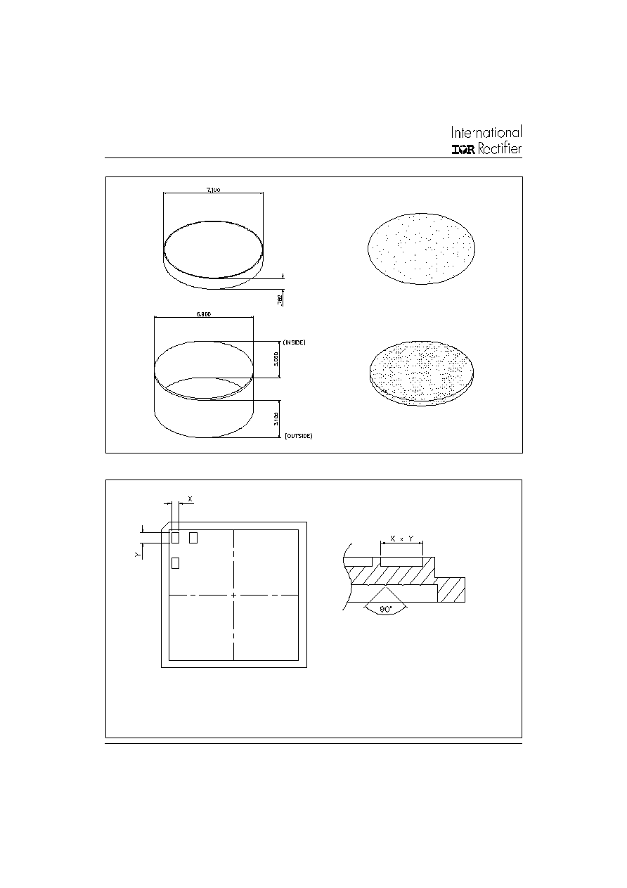
SC
105
H
100
S
5
B
1
2
3
1
-
Schottky Die
2
-
Chip Dimension in Mils
3
-
Process (see Electrical Characteristics Table)
4
-
Voltage code: Code = V
RRM
5
-
Chip surface metallization (see Mechanical Data Table)
6
-
Wafer Diameter in inches
7
-
Packaging (see Packaging Table)
4
Device Code
Ordering Information Table
5
6
7
H = 830 Process
R = OR'ing Process
S = Standard Process
Wafer on Film
STEEL FRAME
SC105.....5. Series
4
Bulletin I0503J 12/99
www.irf.com
Wafer in Box
Die in Waffle Pack
ROUND CONTAINER
FOAM DISK
TYVEK DISK
CHIP TRAY POCKET
SC105.....5. Series
5
Bulletin I0503J 12/99
www.irf.com
WORLD HEADQUARTERS: 233 Kansas St., El Segundo, California 90245 U.S.A. Tel: (310) 322 3331. Fax: (310) 322 3332.
EUROPEAN HEADQUARTERS: Hurst Green, Oxted, Surrey RH8 9BB, U.K. Tel: ++ 44 1883 732020. Fax: ++ 44 1883 733408.
IR CANADA: 15 Lincoln Court, Brampton, Markham, Ontario L6T3Z2. Tel: (905) 453 2200. Fax: (905) 475 8801.
IR GERMANY: Saalburgstrasse 157, 61350 Bad Homburg. Tel: ++ 49 6172 96590. Fax: ++ 49 6172 965933.
IR ITALY: Via Liguria 49, 10071 Borgaro, Torino. Tel: ++ 39 11 4510111. Fax: ++ 39 11 4510220.
IR FAR EAST: K&H Bldg., 2F, 30-4 Nishi-Ikebukuro 3-Chome, Toshima-Ku, Tokyo, Japan 171. Tel: 81 3 3983 0086.
IR SOUTHEAST ASIA: 1 Kim Seng Promenade, Great World City West Tower,13-11, Singapore 237994. Tel: ++ 65 838 4630.
IR TAIWAN: 16 Fl. Suite D.207, Sec. 2, Tun Haw South Road, Taipei, 10673, Taiwan. Tel: 886 2 2377 9936.
http://www.irf.com
Fax-On-Demand: +44 1883 733420 Data and specifications subject to change without notice.
Tape and Reel
BARE DIE CARRIER TAPE
REEL FRAME