 | –≠–ª–µ–∫—Ç—Ä–æ–Ω–Ω—ã–π –∫–æ–º–ø–æ–Ω–µ–Ω—Ç: 30N120 | –°–∫–∞—á–∞—Ç—å:  PDF PDF  ZIP ZIP |

© 2000 IXYS All rights reserved
1 - 4
Symbol
Conditions
Maximum Ratings
V
CES
T
J
= 25∞C to 150∞C
1200
V
V
CGR
T
J
= 25∞C to 150∞C; R
GE
= 20 k
W
1200
V
V
GES
Continuous
±20
V
V
GEM
Transient
±30
V
I
C25
T
C
= 25∞C
60
A
I
C90
T
C
= 90∞C
38
A
I
CM
T
C
= 90∞C, t
p
= 1 ms
76
A
RBSOA
V
GE
= ±15 V, T
J
= 125∞C, R
G
= 47
W
I
CM
= 50
A
Clamped inductive load, L = 30 µH
V
CEK
< V
CES
t
SC
V
GE
= ±15 V, V
CE
= V
CES
, T
J
= 125∞C
10
µs
(SCSOA)
R
G
= 47
W
, non repetitive
P
C
T
C
= 25∞C
IGBT
300
W
Diode
135
W
T
J
-55 ... +150
∞C
T
stg
-55 ... +150
∞C
Maximum lead temperature for soldering
300
∞C
1.6 mm (0.062 in.) from case for 10 s
M
d
Mounting torque
1.1/10 Nm/lb.in.
Weight
6
g
V
CES
= 1200 V
I
C25
= 60 A
V
CE(sat) typ
= 2.4 V
Features
q
NPT IGBT technology
q
low saturation voltage
q
low switching losses
q
square RBSOA, no latch up
q
high short circuit capability
q
positive temperature coefficient for
easy paralleling
q
MOS input, voltage controlled
q
optional ultra fast diode
q
International standard packages
Advantages
q
Space savings
q
High power density
q
IXDT:
surface mountable high power package
Typical Applications
q
AC motor speed control
q
DC servo and robot drives
q
DC choppers
q
Uninteruptible power supplies (UPS)
q
Switch-mode and resonant-mode
power supplies
High Voltage IGBT
with optional Diode
Short Circuit SOA Capability
Square RBSOA
IXDH 30N120
IXDH 30N120 D1
IXDT 30N120
IXDT 30N120 D1
Symbol
Conditions
Characteristic Values
(T
J
= 25∞C, unless otherwise specified)
min.
typ.
max.
V
(BR)CES
V
GE
= 0 V
1200
V
V
GE(th)
I
C
= 1 mA, V
CE
= V
GE
4.5
6.5
V
I
CES
V
CE
= V
CES
T
J
= 25∞C
1.5 mA
T
J
= 125∞C
2.5
mA
I
GES
V
CE
= 0 V, V
GE
= ±
20 V
± 500
nA
V
CE(sat)
I
C
= 30 A, V
GE
= 15 V
2.4
2.9
V
TO-247 AD (IXDH)
G
E
C
C (TAB)
TO--268 AA (IXDT)
G
E
C (TAB)
G = Gate,
E = Emitter
C = Collector ,
TAB = Collector
IXDH 30N120
IXDH 30N120 D1
IXDT
30N120
IXDT
30N120 D1
G
C
E
G
C
E
031
© 2000 IXYS All rights reserved
2 - 4
IXDH 30N120
IXDT 30N120
IXDH 30N120 D1 IXDT 30N120 D1
Symbol
Conditions
Characteristic Values
(T
J
= 25∞C, unless otherwise specified)
min.
typ.
max.
C
ies
1650
pF
C
oes
V
CE
= 25 V, V
GE
= 0 V, f = 1 MHz
250
pF
C
res
110
pF
Q
g
I
C
= 30 A, V
GE
= 15 V, V
CE
= 0.5 V
CES
120
nC
t
d(on)
100
ns
t
r
70
ns
t
d(off)
500
ns
t
f
70
ns
E
on
4.6
mJ
E
off
3.4
mJ
R
thJC
0.42 K/W
R
thCK
Package with heatsink compound
0.25
K/W
Inductive load, T
J
= 125∞C
I
C
= 30 A, V
GE
= ±15 V,
V
CE
= 600 V, R
G
= 47
W
Reverse Diode (FRED) [D1 version only]
Characteristic Values
(T
J
= 25∞C, unless otherwise specified)
Symbol
Conditions
min.
typ.
max.
V
F
I
F
= 30 A, V
GE
= 0 V
2.5
2.7
V
I
F
= 30 A, V
GE
= 0 V, T
J
= 125∞C
2.0
V
I
F
T
C
= 25∞C
60
A
T
C
= 90∞C
35
A
I
RM
I
F
= 30 A, -di
F
/dt = 400 A/µs, V
R
= 600 V
20
A
t
rr
V
GE
= 0 V, T
J
= 125∞C
200
ns
t
rr
I
F
= 1 A, -di
F
/dt = 100 A/µs, V
R
= 30 V, V
GE
= 0 V
40
ns
R
thJC
1 K/W
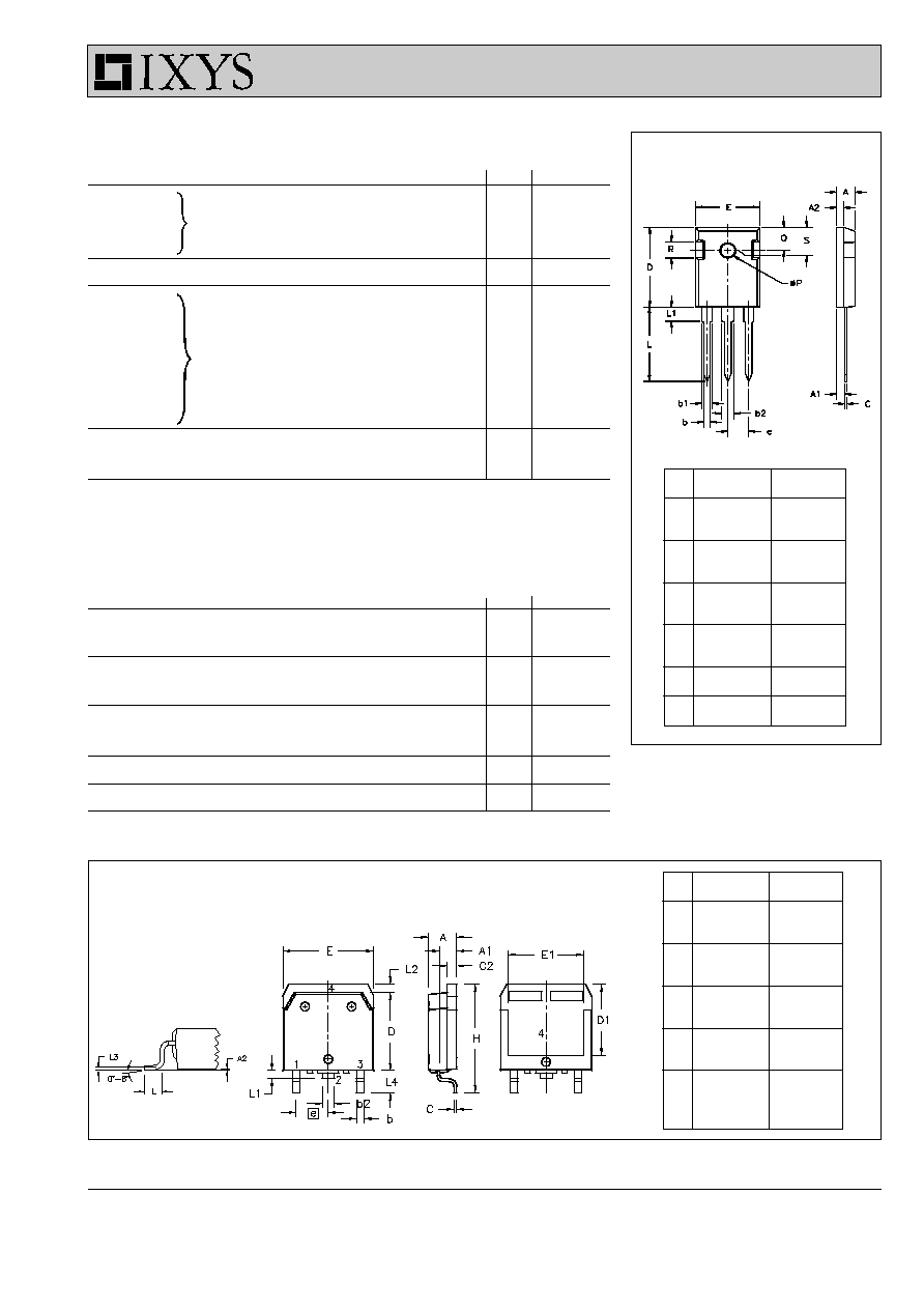
TO-247 AD Outline
Dim.
Millimeter
Inches
Min.
Max.
Min.
Max.
A
4.7
5.3
.185
.209
A
1
2.2
2.54
.087
.102
A
2
2.2
2.6
.059
.098
b
1.0
1.4
.040
.055
b
1
1.65
2.13
.065
.084
b
2
2.87
3.12
.113
.123
C
.4
.8
.016
.031
D
20.80
21.46
.819
.845
E
15.75
16.26
.610
.640
e
5.20
5.72
0.205 0.225
L
19.81
20.32
.780
.800
L1
4.50
.177
∆
P
3.55
3.65
.140
.144
Q
5.89
6.40
0.232 0.252
R
4.32
5.49
.170
.216
S
6.15 BSC
242 BSC
TO-268 AA Outline
Dim.
Millimeter
Inches
Min.
Max.
Min.
Max.
A
4.9
5.1
.193
.201
A
1
2.7
2.9
.106
.114
A
2
.02
.25
.001
.010
b
1.15
1.45
.045
.057
b
2
1.9
2.1
.75
.83
C
.4
.65
.016
.026
D
13.80
14.00
.543
.551
E
15.85
16.05
.624
.632
E
1
13.3
13.6
.524
.535
e 5.45 BSC .215 BSC
H
18.70
19.10
.736
.752
L
2.40
2.70
.094
.106
L1
1.20
1.40
.047
.055
L2
1.00
1.15
.039
.045
L3 0.25 BSC .010 BSC
L4
3.80
4.10
.150
.161
© 2000 IXYS All rights reserved
3 - 4
0
200
400
600
800
1000
0
20
40
60
0
100
200
300
0
1
2
3
4
0
10
20
30
40
50
60
70
80
0.0
0.5
1.0
1.5
2.0
2.5
3.0
0
10
20
30
40
50
60
0
20
40
60
80
100 120 140
0
5
10
15
20
0.0
0.5
1.0
1.5
2.0
2.5
3.0
3.5
0
10
20
30
40
50
60
13V
11V
T
J
= 25∞C
V
GE
=17V
T
J
= 125∞C
V
CE
= 600V
I
C
= 25A
15V
5
6
7
8
9
10
11
0
10
20
30
40
50
60
13V
11V
V
GE
=17V
15V
V
CE
= 20V
T
J
= 25∞C
9V
9V
V
CE
V
A
I
C
V
CE
A
I
C
V
V
V
V
GE
V
F
A
I
C
A
I
F
nC
Q
G
-di/dt
V
V
GE
A
I
RM
t
rr
ns
A/
m
s
IXDH30N120
T
J
= 125∞C
V
R
= 600V
I
F
= 30A
T
J
= 25∞C
T
J
= 125∞C
I
RM
t
rr
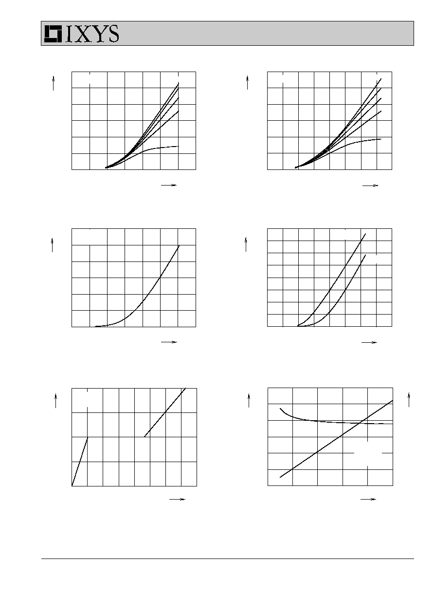
Fig. 1 Typ. output characteristics
Fig. 2 Typ. output characteristics
Fig. 3 Typ. transfer characteristics
Fig. 4 Typ. forward characteristics of
free wheeling diode
Fig. 5 Typ. turn on gate charge
Fig. 6 Typ. turn off characteristics of
free wheeling diode
IXDH 30N120
IXDT 30N120
IXDH 30N120 D1 IXDT 30N120 D1

© 2000 IXYS All rights reserved
4 - 4
Fig. 7 Typ. turn on energy and switching
Fig. 8 Typ. turn off energy and switching
times versus collector current
times versus collector current
Fig. 9 Typ. turn on energy and switching
Fig.10 Typ. turn off energy and switching
times versus gate resistor
times versus gate resistor
Fig. 11 Reverse biased safe operating area
Fig. 12 Typ. transient thermal impedance
RBSOA
0
10
20
30
40
50
0
2
4
6
8
10
12
14
0
20
40
60
80
100
120
140
0
10
20
30
40
50
0
1
2
3
4
5
6
0
100
200
300
400
500
600
0.00001
0.0001
0.001
0.01
0.1
1
0.0001
0.001
0.01
0.1
1
10
0
40
80
120
160
200
240
0
1
2
3
4
5
0
300
600
900
1200
1500
0
40
80
120
160
200
240
0
2
4
6
8
10
12
0
60
120
180
240
single pulse
V
CE
= 600V
V
GE
= ±15V
R
G
= 47
W
T
J
= 125∞C
IXDH30N120
V
CE
= 600V
V
GE
= ±15V
I
C
= 25A
T
J
= 125∞C
0
200
400
600
800
1000 1200
0
10
20
30
40
50
60
R
G
= 47
W
T
J
= 125∞C
V
CEK
< V
CES
V
CE
= 600V
V
GE
= ±15V
R
G
= 47
W
T
J
= 125∞C
E
on
V
CE
= 600V
V
GE
= ±15V
I
C
= 25A
T
J
= 125∞C
t
d(on)
t
r
E
off
t
d(off)
t
f
E
on
t
d(on)
t
r
E
off
t
d(off)
t
f
I
C
A
I
C
A
E
off
E
on
t
t
R
G
W
R
G
W
V
CE
t
s
mJ
E
on
mJ
E
off
ns
t
ns
t
I
CM
K/W
Z
thJC
IGBT
diode
V
A
mJ
ns
ns
mJ
IXDH 30N120
IXDT 30N120
IXDH 30N120 D1 IXDT 30N120 D1