Äîêóìåíòàöèÿ è îïèñàíèÿ www.docs.chipfind.ru
1 - 5
© 2000 IXYS All rights reserved
Symbol
Test Conditions
Characteristic Values
(T
J
= 25
°
C, unless otherwise specified)
Min.
Typ.
Max.
BV
CES
I
C
= 3 mA, V
GE
= 0 V
1000
V
BV
CES
temperature coefficient 0.072
%/K
V
GE(th)
I
C
= 500
m
A, V
GE
= V
GE
2.5
5.5
V
V
GE(th)
temperature coefficient -0.192
%/K
I
CES
V
CE
= 0.8, V
CES
T
J
= 25
°
C
300
m
A
V
GE
= 0 V
T
J
= 125
°
C
5
mA
I
GES
V
CE
= 0 V, V
GE
=
±
20 V
±
100
nA
V
CE(sat)
I
C
= I
CE90
, V
GE
= 15
12N100U1
3.5
V
12N100AU1
4.0
V
Features
· International standard packages
JEDEC TO-247
· IGBT with antiparallel FRED in one
package
· HDMOS
TM
process
· Low V
CE(sat)
- for minimum on-state conduction
losses
· MOS Gate turn-on
- drive simplicity
· Fast Recovery Expitaxial Diode (FRED)
- soft recovery with low I
RM
Applications
· DC choppers
· AC motor speed control
· DC servo and robot drives
· Uninterruptible power supplies (UPS)
· Switch-mode and resonant-mode
power supplies
Advantages
· Easy to mount with one screw
· Reduces assembly time and cost
· Space savings (two devices in one
package)
95596C (7/00)
Low V
CE(sat)
IGBT with Diode
High Speed IGBT with Diode
Combi Pack
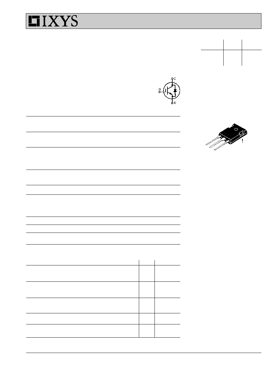
G = Gate
C
= Collector
E = Emitter
TAB = Collector
G
C
E
C (TAB)
TO-247AD
Symbol
Test Conditions
Maximum Ratings
V
CES
T
J
= 25
°
C to 150
°
C
1000
V
V
CGR
T
J
= 25
°
C to 150
°
C; R
GE
= 1 M
W
1000
V
V
GES
Continuous
±
20
V
V
GEM
Transient
±
30
V
I
C25
T
C
= 25
°
C
24
A
I
C90
T
C
= 90
°
C
12
A
I
CM
T
C
= 25
°
C, 1 ms
48
A
SSOA
V
GE
= 15 V, T
VJ
= 125
°
C, R
G
= 150
W
I
CM
= 24
A
(RBSOA)
Clamped inductive load, L = 300
m
H
@ 0.8 V
CES
P
C
T
C
= 25
°
C
100
W
T
J
-55 ... +150
°
C
T
JM
150
°
C
T
stg
-55 ... +150
°
C
M
d
Mounting torque with screw M3
1.13/10 Nm/lb.in.
Weight
6
g
Maximum lead temperature for soldering
300
°
C
1.6 mm (0.062 in.) from case for 10 s
V
CES
I
C25
V
CE(sat)
IXGH 12N100U1
1000 V 24 A 3.5 V
IXGH 12N100AU1
1000 V 24 A 4.0 V
IXYS reserves the right to change limits, test conditions, and dimensions.
2 - 5
© 2000 IXYS All rights reserved
Reverse Diode (FRED)
Characteristic Values
(T
J
= 25
°
C, unless otherwise specified)
Symbol
Test Conditions
Min. Typ. Max.
V
F
I
F
=8A, V
GE
= 0 V,
2.75
V
Pulse test, t
£
300
m
s, duty cycle d
£
2 %
I
RM
I
F
= I
C90
, V
GE
= 0 V, -di
F
/dt = 100 A/
m
s
6.5
A
t
rr
V
R
= 540 V
T
J
= 125
°
C
120
ns
I
F
= 1 A, -di/dt = 50 A/
m
s, V
R
= 30 V
T
J
= 25
°
C
50
60
ns
R
thJC
2.5
K/W
Inductive load, T
J
= 125
°
C
I
C
= I
C90
, V
GE
= 15 V, L = 300
m
H
V
CE
= 800 V, R
G
= R
off
= 120
W
Remarks: Switching times may
increase for V
CE
(Clamp) > 0.8 V
CES
,
higher T
J
or increased R
G
Inductive load, T
J
= 25
°
C
I
C
= I
C90
, V
GE
= 15 V, L = 300
m
H
V
CE
= 800 V, R
G
= R
off
= 120
W
Remarks: Switching times may
increase for V
CE
(Clamp) > 0.8 V
CES
,
higher T
J
or increased R
G
Symbol
Test Conditions
Characteristic Values
(T
J
= 25
°
C, unless otherwise specified)
Min. Typ.
Max.
g
fs
I
C
= I
C90
; V
CE
= 10 V,
6
10
S
Pulse test, t
£
300
m
s, duty cycle
£
2 %
C
ies
750
pF
C
oes
V
CE
= 25 V, V
GE
= 0 V, f = 1MHz
120
pF
C
res
30
pF
Q
g
65
90
nC
Q
ge
I
C
= I
C90
, V
GE
= 15 V, V
CE
= 0.5 V
CES
8
20
nC
Q
gc
24
45
nC
t
d(on)
100
ns
t
ri
200
ns
t
d(off)
850 1000
ns
t
fi
12N100U1
800 1000
ns
12N100AU1
500
700
ns
E
off
12N100U1
2.5
mJ
12N100AU1
1.5
3.0
mJ
t
d(on)
100
ns
t
ri
200
ns
E
(on)
1.1
mJ
t
d(off)
900
ns
t
fi
12N100U1
1250
ns
12N100AU1
950
ns
E
off
12N100U1
3.5
mJ
12N100AU1
2.2
mJ
R
thJC
1.25
K/W
R
thCK
0.25
K/W
IXGH12N100U1
IXGH12N100AU1
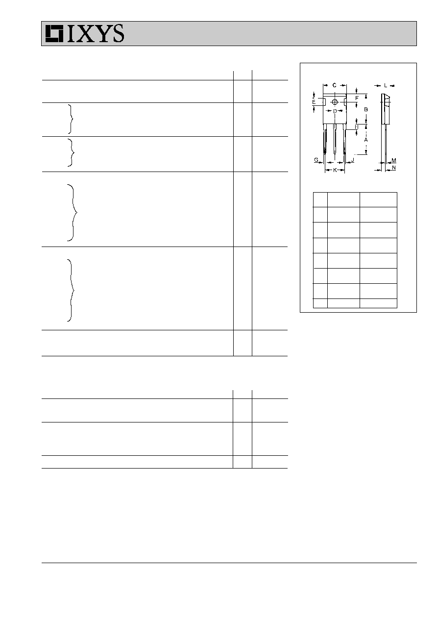
TO-247 AD (IXGH) Outline
Dim. Millimeter
Inches
Min.
Max.
Min.
Max.
A
19.81 20.32
0.780 0.800
B
20.80 21.46
0.819 0.845
C
15.75 16.26
0.610 0.640
D
3.55
3.65
0.140 0.144
E
4.32
5.49
0.170 0.216
F
5.4
6.2
0.212 0.244
G
1.65
2.13
0.065 0.084
H
-
4.5
-
0.177
J
1.0
1.4
0.040 0.055
K
10.8
11.0
0.426 0.433
L
4.7
5.3
0.185 0.209
M
0.4
0.8
0.016 0.031
N
1.5
2.49
0.087 0.102
IXYS MOSFETS and IGBTs are covered by one or more of the following U.S. patents:
4,835,592
4,881,106
5,017,508
5,049,961
5,187,117
5,486,715
4,850,072
4,931,844
5,034,796
5,063,307
5,237,481
5,381,025
3 - 5
© 2000 IXYS All rights reserved
V
GE
- Volts
2
4
6
8
10
12
I
C
- A
m
pe
r
e
s
0
10
20
30
40
50
V
CE
- Volts
0
2
4
6
8
10
I
C
-
A
m
p
e
r
e
s
0
10
20
30
40
50
V
CE
-Volts
0
5
10
15
20
25
30
35
40
Ca
pac
i
ta
nc
e -
p
F
10
100
1000
T
J
- Degrees C
25
50
75
100
125
150
V
C
E
(
sat
)
-
N
o
rm
a
l
iz
ed
0.6
0.8
1.0
1.2
1.4
1.6
V
CE
- Volts
0
4
8
12
16
20
I
C
-
A
m
pe
r
e
s
0
20
40
60
80
100
13V
11V
9V
7V
V
CE
= 10V
T
J
= 25°C
V
GE
= 15V
T
J
= 25°C
I
C
= 6A
I
C
= 12A
I
C
= 24A
f = 1Mhz
7V
V
GE
= 15V
T
J
= 25°C
V
CE
- Volts
0
2
4
6
8
10
I
C
- A
m
pe
r
e
s
0
10
20
30
40
50
T
J
= 125°C
C
iss
C
oss
V
GE
= 15V
13V
11V
V
GE
= 15V
13V
11V
9V
7V
9V
C
rss
T
J
=
125°C
IXGH12N100U1
IXGH12N100AU1
Figure 4. Temperature Dependence of V
CE(sat)
Figure 2. Extended Output Characteristics
Figure 1. Saturation Voltage Characteristics
Figure 3. Saturation Voltage Characteristics
Figure 6. Capacitance Curves
Figure 5. Admittance Curves
4 - 5
© 2000 IXYS All rights reserved
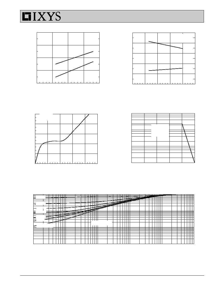
Pulse Width - Seconds
0.00001
0.0001
0.001
0.01
0.1
1
Z
th
JC
(K/W)
0.001
0.01
0.1
1
V
CE
- Volts
0
200
400
600
800
1000
I
C
- A
m
p
e
re
s
0.1
1
10
100
Q
g
- nanocoulombs
0
15
30
45
60
75
V
GE
-
Vo
lts
0
3
6
9
12
15
R
G
- Ohms
0
30
60
90
120
150
E
(O
FF
)
-
m
illijoule
s
0
1
2
3
4
5
t
fi
- na
no
se
co
nd
s
0
200
400
600
800
1000
I
C
- Amperes
0
5
10
15
20
E
(O
FF
)
- m
illiJ
oule
s
1
2
3
4
5
t
fi
-
na
no
se
co
nd
s
800
900
1000
1100
1200
V
CE
= 150V
I
C
= 30A
t
fi
E
(OFF)
T
J
= 125°C
R
G
= 4.7
dV/dt < 5V/ns
D=0.5
D=0.1
D=0.05
D=0.01
Single pulse
D = Duty Cycle
R
G
= 120
T
J
= 125°C
24
T
J
= 125°C
E
(OFF)
D=0.2
D=0.02
I
C
= 12A
t
fi
IXGH12N100U1
IXGH12N100AU1
Figure 7. Dependence of tfi and E
OFF
on I
C
.
Figure 11. Transient Thermal Resistance
Figure 8. Dependence of tfi and E
OFF
on R
G
.
Figure 9. Gate Charge
Figure 10. Turn-off Safe Operating Area
5 - 5
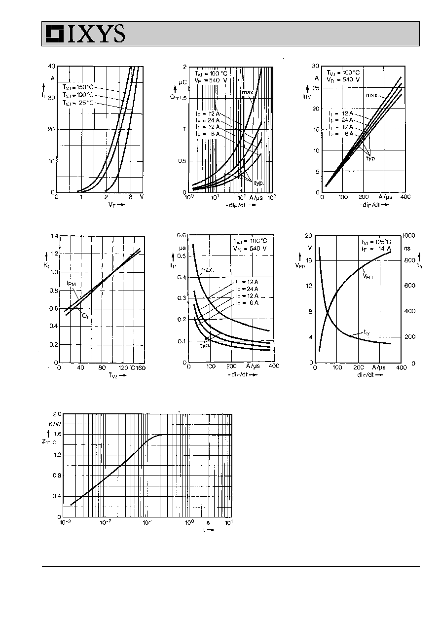
© 2000 IXYS All rights reserved
IXGH12N100U1
IXGH12N100AU1
Fig. 12. Forward current versus
Fig. 13. Recovery charge versus -di
F
/dt.
Fig. 14. Peak reverse current versus
voltage drop.
-di
F
/dt.
Fig. 15. Dynamic parameters versus
Fig. 16. Reverse recovery time .
Fig. 17. Forward voltage recovery and
junction temperature.
versus -di
F
/dt
time versus -di
F
/dt.
Fig. 18. Transient thermal impedance junction to case.