©1997 IXYS Corporation. All rights reserved.
Symbol
Test Conditions
Maximum Ratings
V
CES
T
J
= 25
∞
C to 150
∞
C
600
V
V
CGR
T
J
= 25
∞
C to 150
∞
C; R
GE
= 1 M
600
V
V
GES
Continuous
±
20
V
V
GEM
Transient
±
30
V
I
C25
T
C
= 25
∞
C
48
A
I
C90
T
C
= 90
∞
C
24
A
I
CM
T
C
= 25
∞
C, 1 ms
96
A
SSOA
V
GE
= 15 V, T
VJ
= 125
∞
C, R
G
= 22
I
CM
= 48
A
(RBSOA)
Clamped inductive load, L = 100
µ
H
@ 0.8 V
CES
P
C
T
C
= 25
∞
C
150
W
T
J
-55 ... +150
∞
C
T
JM
150
∞
C
T
stg
-55 ... +150
∞
C
Maximum Lead and Tab temperature for soldering
300
∞
C
1.6 mm (0.062 in.) from case for 10 s
M
d
Mounting torque, TO-247 AD
1.13/10 Nm/lb.in.
Weight
TO-247 SMD
4
g
TO-247 AD
6
g
Features
l
International standard packages
JEDEC TO-247 SMD surface
mountable and JEDEC TO-247 AD
l
IGBT and anti-parallel FRED in one
package
l
2nd generation HDMOS
TM
process
l
Low V
CE(sat)
- for minimum on-state conduction
losses
l
MOS Gate turn-on
- drive simplicity
l
Fast Recovery
Epitaxial Diode (FRED)
- soft recovery with low I
RM
Applications
l
AC motor speed control
l
DC servo and robot drives
l
DC choppers
l
Uninterruptible power supplies (UPS)
l
Switch-mode and resonant-mode
power supplies
Advantages
l
Space savings (two devices in one
package)
l
Easy to mount with 1 screw, TO-247
(isolated mounting screw hole)
l
Reduces assembly time and cost
Symbol
Test Conditions
Characteristic Values
(T
J
= 25
∞
C, unless otherwise specified)
min.
typ.
max.
BV
CES
I
C
= 750
µ
A, V
GE
= 0 V
600
V
V
GE(th)
I
C
= 250
µ
A, V
CE
= V
GE
2.5
5.5
V
I
CES
V
CE
= 0.8 ∑ V
CES
T
J
= 25
∞
C
500
µ
A
V
GE
= 0 V
T
J
= 125
∞
C
8
mA
I
GES
V
CE
= 0 V, V
GE
=
±
20 V
±
100
nA
V
CE(sat)
I
C
= I
C90
, V
GE
= 15 V
2.7
V
G
C
E
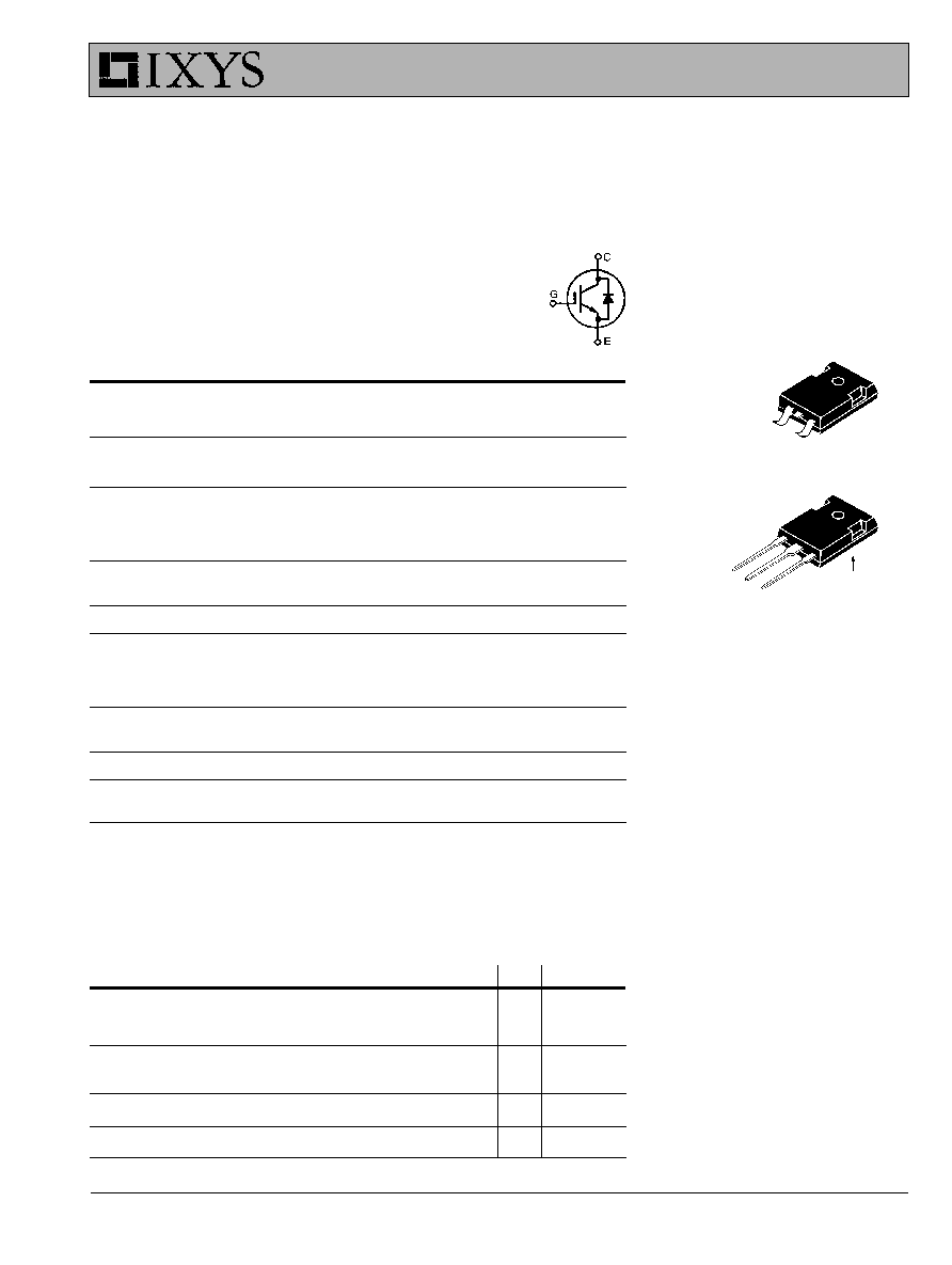
TO-247 AD
(24N60AU1)
G = Gate,
C = Collector,
E = Emitter,
TAB = Collector
C (TAB)
G
E
C (TAB)
TO-247 SMD
(24N60AU1S)
V
CES
=
600 V
I
C25
=
48 A
V
CE(sat)
=
2.7 V
t
fi
= 275 ns
HiPerFAST
TM
IGBT with Diode
Combi Pack
IXGH
24N60AU1
IXGH
24N60AU1S
92717H (3/97)

IXYS MOSFETS and IGBTs are covered by one or more of the following U.S. patents:
4,835,592
4,881,106
5,017,508
5,049,961
5,187,117
5,486,715
4,850,072
4,931,844
5,034,796
5,063,307
5,237,481
5,381,025
IXYS reserves the right to change limits, test conditions, and dimensions.
IXGH24N60AU1
IXGH24N60AU1S
1. Gate
2. Collector
3. Emitter
4. Collector
Dim.
Millimeter
Inches
Min.
Max.
Min.
Max.
A
4.83
5.21
.190
.205
A1
2.29
2.54
.090
.100
A2
1.91
2.16
.075
.085
b
1.14
1.40
.045
.055
b1
1.91
2.13
.075
.084
C
0.61
0.80
.024
.031
D
20.80
21.34
.819
.840
E
15.75
16.13
.620
.635
e
5.45
BSC
.215
BSC
L
4.90
5.10
.193
.201
L1
2.70
2.90
.106
.114
L2
2.10
2.30
.083
.091
L3
0.00
0.10
.00
.004
L4
1.90
2.10
.075
.083
ÿP
3.55
3.65
.140
.144
Q
5.59
6.20
.220
.244
R
4.32
4.83
.170
.190
S
6.15
BSC
.242
BSC
TO-247 SMD Outline
TO-247 AD Outline
Dim.
Millimeter
Inches
Min.
Max.
Min.
Max.
A
4.7
5.3
.185
.209
A
1
2.2
2.54
.087
.102
A
2
2.2
2.6
.059
.098
b
1.0
1.4
.040
.055
b
1
1.65
2.13
.065
.084
b
2
2.87
3.12
.113
.123
C
.4
.8
.016
.031
D
20.80
21.46
.819
.845
E
15.75
16.26
.610
.640
e
5.20
5.72
0.205 0.225
L
19.81
20.32
.780
.800
L1
4.50
.177
P
3.55
3.65
.140
.144
Q
5.89
6.40
0.232 0.252
R
4.32
5.49
.170
.216
S
6.15 BSC
242 BSC
e
P
Symbol
Test Conditions
Characteristic Values
(T
J
= 25
∞
C, unless otherwise specified)
min.
typ.
max.
g
fs
I
C
= I
C90
; V
CE
= 10 V,
9
13
S
Pulse test, t
300
µ
s, duty cycle
2 %
C
ies
1500
pF
C
oes
V
CE
= 25 V, V
GE
= 0 V, f = 1 MHz
175
pF
C
res
40
pF
Q
g
90
120
nC
Q
ge
I
C
= I
C90
, V
GE
= 15 V, V
CE
= 0.5 V
CES
11
15
nC
Q
gc
30
40
nC
t
d(on)
25
ns
t
ri
15
ns
E
on
0.6
mJ
t
d(off)
150
200
ns
t
fi
110
270
ns
E
off
1.5
mJ
t
d(on)
25
ns
t
ri
15
ns
E
on
0.8
mJ
t
d(off)
250
ns
t
fi
400
ns
E
off
2.3
mJ
R
thJC
0.83 K/W
R
thCK
0.25
K/W
Inductive load, T
J
= 125
∞∞
∞∞
∞
C
I
C
= I
C90
, V
GE
= 15 V, L = 100
µ
H
V
CE
= 0.8 V
CES
, R
G
= R
off
= 10
Remarks: Switching times may increase
for V
CE
(Clamp) > 0.8 ∑ V
CES
, higher T
J
or
increased R
G
Inductive load, T
J
= 25
∞∞
∞∞
∞
C
I
C
= I
C90
, V
GE
= 15 V, L = 100
µ
H,
V
CE
= 0.8 V
CES
, R
G
= R
off
= 10
Remarks: Switching times may increase
for V
CE
(Clamp) > 0.8 ∑ V
CES
, higher T
J
or
increased R
G
Min. Recommended Footprint (Dimensions in inches and (mm))
Reverse Diode (FRED)
Characteristic Values
(T
J
= 25
∞
C, unless otherwise specified)
Symbol
Test Conditions
min.
typ.
max.
V
F
I
F
= I
C90
, V
GE
= 0 V,
1.6
V
Pulse test, t
300
µ
s, duty cycle d
2 %
I
RM
I
F
= I
C90
, V
GE
= 0 V, -di
F
/dt = 240 A/
µ
s
10
15
A
t
rr
V
R
= 360 V
T
J
= 125
∞
C
150
ns
I
F
= 1 A; -di/dt = 100 A/
µ
s; V
R
= 30 VT
J
= 25
∞
C
35
50
ns
R
thJC
1 K/W

©1997 IXYS Corporation. All rights reserved.
G20N60p1.JNB
T
J
- Degrees C
-50
-25
0
25
50
75
100 125 150
BV
/
V
GE
(
t
h
)
- N
o
r
m
ali
ze
d
0.6
0.7
0.8
0.9
1.0
1.1
1.2
T
J
- Degrees C
-50
-25
0
25
50
75
100 125 150
V
CE
(
s
a
t
)
- N
o
rm
al
ize
d
0.4
0.6
0.8
1.0
1.2
1.4
1.6
V
CE
- Volts
0
1
2
3
4
5
6
7
I
C
- Am
per
e
s
0
5
10
15
20
25
30
35
40
7V
9V
13V
11V
V
GE
- Volts
5
6
7
8
9
10
11
12 13
14
15
V
CE
-
V
olts
0
1
2
3
4
5
6
7
8
9
10
V
GE
- Volts
3
4
5
6
7
8
9
10
I
C
- A
m
pe
re
s
0
5
10
15
20
25
30
35
40
V
CE
- Volts
0
2
4
6
8
10
12
14
16
18
20
I
C
- A
m
pe
re
s
0
25
50
75
100
125
150
13V
11V
9V
7V
T
J
= 25∞C
V
GE
= 15V
V
GE
= 15V
T
J
= 25∞C
I
C
= 10A
I
C
= 40A
I
C
= 20A
T
J
= 25∞C
I
C
= 10A
I
C
= 20A
I
C
= 40A
V
GE
= 15V
T
J
= - 40∞C
V
CE
= 10V
I
C
= 250µA
I
C
= 250µA
V
GE(th)
BV
CES
T
J
= 25∞C
T
J
= 125∞C
Fig. 3 Collector-Emitter Voltage
Fig. 4 Temperature Dependence
vs. Gate-Emitter Voltage
of Output Saturation Voltage
Fig. 5 Input Admittance
Fig. 6 Temperature Dependence of
Breakdown and Threshold Voltage
Fig. 1 Saturation Characteristics
Fig. 2 Output Characterstics
IXGH24N60AU1
IXGH24N60AU1S

IXYS MOSFETS and IGBTs are covered by one or more of the following U.S. patents:
4,835,592
4,881,106
5,017,508
5,049,961
5,187,117
5,486,715
4,850,072
4,931,844
5,034,796
5,063,307
5,237,481
5,381,025
IXYS reserves the right to change limits, test conditions, and dimensions.
IXGH24N60AU1
IXGH24N60AU1S
Pulse Width - seconds
0.0001
0.001
0.01
0.1
1
10
Z
th
j
c
(
K/W
)
0.01
0.1
1
D=0.1
D=0.2
D=0.5
V
CE
- Volts
0
100
200
300
400
500
600
I
C
- A
m
pe
re
s
0.01
0.1
1
10
100
Q
g
- nanocoulombs
0
25
50
75
100
V
GE
- V
olt
s
0
3
6
9
12
15
I
C
= 24A
V
CE
= 300V
R
G
- Ohms
0
20
40
60
80
100
120
E
of
f
-
mi
llijo
ul
es
0
1
2
3
4
5
t
fi
- na
no
se
co
nd
s
0
100
200
300
400
500
E
off
t
fi
I
C
- Amperes
0
10
20
30
40
50
E
of
f
-
mi
llijo
ul
es
0
1
2
3
4
5
t
fi
- na
no
se
co
nd
s
0
100
200
300
400
500
E
off
t
fi
T
J
=
125∞C
R
G
= 10
T
J
=
125∞C
I
C
= 24A
T
J
= 125∞C
R
G
= 10
D=0.05
D=0.02
Single Pulse
D=0.01
G24N60P2.JNB
D = Duty Cycle
Fig.11 Transient Thermal Impedance
Fig.9 Gate Charge Characteristic Curve
Fig.10 Turn-Off Safe Operating Area
Fig.7 Turn-Off Energy per Pulse and
Fig.8 Dependence of Turn-Off Energy
Fall Time on Collector Current
Per Pulse and Fall Time on R
G
dV/dt < 3V/ns

©1997 IXYS Corporation. All rights reserved.
Fig.16 Peak Reverse Recovery Current
Fig.17 Reverse Recovery Time
di
F
/dt - A/µs
0
200
400
600
t
rr
-
na
nos
ec
on
ds
0.0
0.2
0.4
0.6
0.8
di
F
/dt - A/µs
200
400
600
I
RM
-
Am
p
ere
s
0
10
20
30
40
di
F
/dt - A/µs
1
10
100
1000
Q
r
-
na
no
co
u
lom
b
s
0
1
2
3
4
T
J
- Degrees C
0
40
80
120
160
N
o
rm
ali
ze
d I
RM
/Q
r
0.0
0.2
0.4
0.6
0.8
1.0
1.2
1.4
Q
r
I
RM
di
F
/dt - A/µs
0
100
200
300
400
500
600
t
fr
-
na
nos
ec
on
ds
0
200
400
600
800
1000
V
FR
-
Vo
lts
0
5
10
15
20
25
t
fr
V
FR
Voltage Drop - Volts
0.5
1.0
1.5
2.0
2.5
C
u
rre
nt
- A
m
pe
re
s
0
20
40
60
80
100
T
J
= 150∞C
T
J
= 100∞C
T
J
= 25∞C
T
J
= 125∞C
I
F
= 37A
typ.
I
F
= 60A
I
F
= 30A
I
F
= 15A
I
F
= 30A
T
J
= 100∞C
V
R
= 350V
T
J
= 100∞C
V
R
= 350V
T
J
= 100∞C
V
R
= 350V
typ.
I
F
= 60A
I
F
= 30A
I
F
= 15A
max.
I
F
= 30A
max.
I
F
= 30A
typ.
I
F
= 60A
I
F
= 30A
I
F
= 15A
max.
Fig.12 Maximum Forward Voltage Drop
Fig.13 Peak Forward Voltage V
FR
and
Forward Recovery Time t
FR
Fig.14 Junction Temperature Dependence
Fig.15 Reverse Recovery Chargee
off I
RM
and Q
r
IXGH24N60AU1
IXGH24N60AU1S