
2005. 10. 26
1/5
SEMICONDUCTOR
TECHNICAL DATA
KIA431S/AS/BS
BIPOLAR LINEAR INTEGRATED CIRCUIT
Revision No : 1
PROGRAMMABLE PRECISION REFERENCES
The KIA431S/AS/BS integrated circuits are three-terminal
programmable shunt regulator diodes. These monolithic IC voltage
reference operate as a low temperature coefficient zener which is
programmable from V
ref
to 20 volts with two external resistors.
These devices exhibit a wide operating current range of 1.0 to 100mA
with a typical dynamic impedance of 0.22 . The characteristics of
these references make them excellent replacements for zener diodes in
many applications such as digital voltmeters, power supplies, and op
amp circuitry. The 2.5 volt reference makes it convenient to obtain a
stable reference from 5.0 volt logic supplies, and since the
KIA431S/AS/BS operates as a shunt regulator, it can be used
as either a positive or negative voltage reference.
FEATURES
Programmable Output Voltage to 20 Volts.
Low Dynamic Output Impedance : 0.22 (Typ.).
Sink Current Capability of 1.0 to 100mA.
Equivalent Full-Range Temperature Coefficient of 50ppm/
(Typ.).
Temperature Compensated for Operation Over Full Rated
Operating Temperature Range.
Low Output Noise Voltage.
DIM
MILLIMETERS
A
B
D
E
TSM
2.9 0.2
1.6+0.2/-0.1
0.70 0.05
0.4 0.1
2.8+0.2/-0.3
1.9 0.2
0.95
0.16 0.05
0.00-0.10
0.25+0.25/-0.15
C
F
G
H
I
J
K
0.60
L
0.55
A
F
G
G
D
K
B
E
C
L
H
J
J
I
2
1
3
+
_
+
_
+
_
+
_
+
_
1. CATHODE
2. REFERENCE
3.ANODE
Note) * : Under development
Type No.
Marking
KIA431S
3A
KIA431AS
3B
KIA431BS
3C
ITEM
Vref Tolerance (%)
KIA431S
2.2
KIA431AS
1.0
* KIA431BS
0.5
Marking

2005. 10. 26
2/5
KIA431S/AS/BS
Revision No : 1
ELECTRICAL CHARACTERISTICS (Ta=25 )
MAXIMUM RATINGS (Ta=25 )
CHARACTERISTIC
SYMBOL
RATING
UNIT
Cathode To Anode Voltage
V
KA
20
V
Cathode Current Range, Continuous
I
K
-100 150
mA
Reference Input Current Range, Continuous
I
ref
-0.05 10
mA
Operating Junction Temperature
T
j
150
Operating Temperature
T
opr
-40 85
Storage Temperature
T
stg
-65 150
Total Power Dissipation (Note)
P
D
900
mW
CHARACTERISTICS
SYMBOL
TEST
CIRCUIT
TEST CONDITION
MIN.
TYP.
MAX. UNIT
Reference Input
Voltage
KIA431S
V
ref
Figure 1
V
KA
=V
ref
, I
K
=10mA
2.440
2.495
2.550
V
KIA431AS
2.470
2.495
2.520
V
KIA431BS
2.4825 2.495 2.5075
V
Reference Input Voltage
Deviation Over Temperature Range
V
ref
Figure 1
(Note 1)
V
KA
=V
ref
, I
K
=10mA
-
7.0
30
mV
Ratio of Change in Reference Input
Voltage to Change in Cathode to
Anode Voltage
V
ref
/
V
KA
Figure 2
I
K
=10mA
V
KA
=
10V V
ref
-
-1.4
-2.7
mV/V
V
KA
=
20V 10V
-
-1.0
-2.0
Reference Input Current
Ta=25
I
ref
Figure 2
I
K
=10mA, R1=10k , R2=
-
1.8
4.0
A
Ta=T
opr
-
-
6.5
Reference Input Current
Deviation Over Temperature Range
I
ref
Figure 2
I
K
=10mA, R1=10k , R2=
-
0.8
2.5
A
Minimum Cathode Current For Regulation
I
min
Figure 1
V
KA
=V
ref
-
0.5
1.0
mA
Off-State Cathode Current
I
off
Figure 3
V
KA
=20V, V
ref
=0V
-
2.6
1000
nA
Dynamic Impedance
Z
ka
Figure 1
(Note 2)
V
KA
=V
ref
, I
K
=1.0 100mA,
f 1.0kHz
-
0.22
-
Reference
(R)
Anode(A)
Cathode
(K)
(K)
Cathode
Anode(A)
Reference
(R)
2.5V
ref
+
-
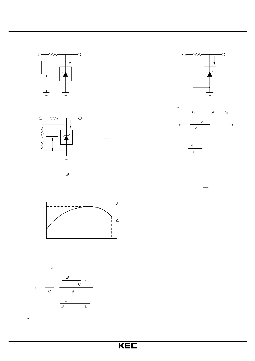
BLOCK DIAGRAM
Note) Package mounted on a ceramic board. (600m
2
0.8m)
2005. 10. 26
3/5
KIA431S/AS/BS
Revision No : 1
Input
V
KA
I
K
V
ref
FIGURE 1-TEST CIRCUIT FOR V
KA
= V
ref
off
I
KA
V
Input
FIGURE 3-TEST CIRCUIT FOR I
off
ref
V
>
KA
V
FIGURE 2-TEST CIRCUIT FOR
K
I
KA
V
Input
R1
R2
I
ref
V
ref
V
KA
=
ref
V
( 1+
R1
R2
) + I x
ref
R1
ref
V
Max.
V
ref
Min.
T1
T2
AMBIENT TEMPERATURE
V
ref
= V
ref
(Max.)
ref
V
(Min.)
Ta = T
2
-
-
T
1
Example : V
ref
= 8.0mV and slope is positive,
V
ref
at 25 =2.495V, Ta=70
0.008 10
6
V
ref
= = 45.8 ppm/
70 (2.495)
Note 2: The dynamic impedance Z
ka
is defined as:
VKA
|Z
ka
| =
Ik
When the device is programmed with two external
resistors, R1 and R2, (refer to Figure 2) the total
dynamic impedance of the circuit is defined as:
R1
|Z
ka'
| = |Z
ka
| (1+ )
R2
Note 1:
The deviation parameter V
ref
is defined as the differences
between the maximum and minimum values obtained over the
full operating ambient temperature range that applies.
The average temperature coefficient of the Reference
input voltage, V
ref
, is defined as:
V
ref
( )
10
6
ppm V
ref
at 25
V
ref
( ) =
Ta
V
ref
10
6
=
Ta(V
ref
at 25 )
V
ref
can be positive or negative depending on whether
V
ref
Min. or V
ref
Max. occurs at the lower ambient temperature.
2005. 10. 26
4/5
KIA431S/AS/BS
Revision No : 1
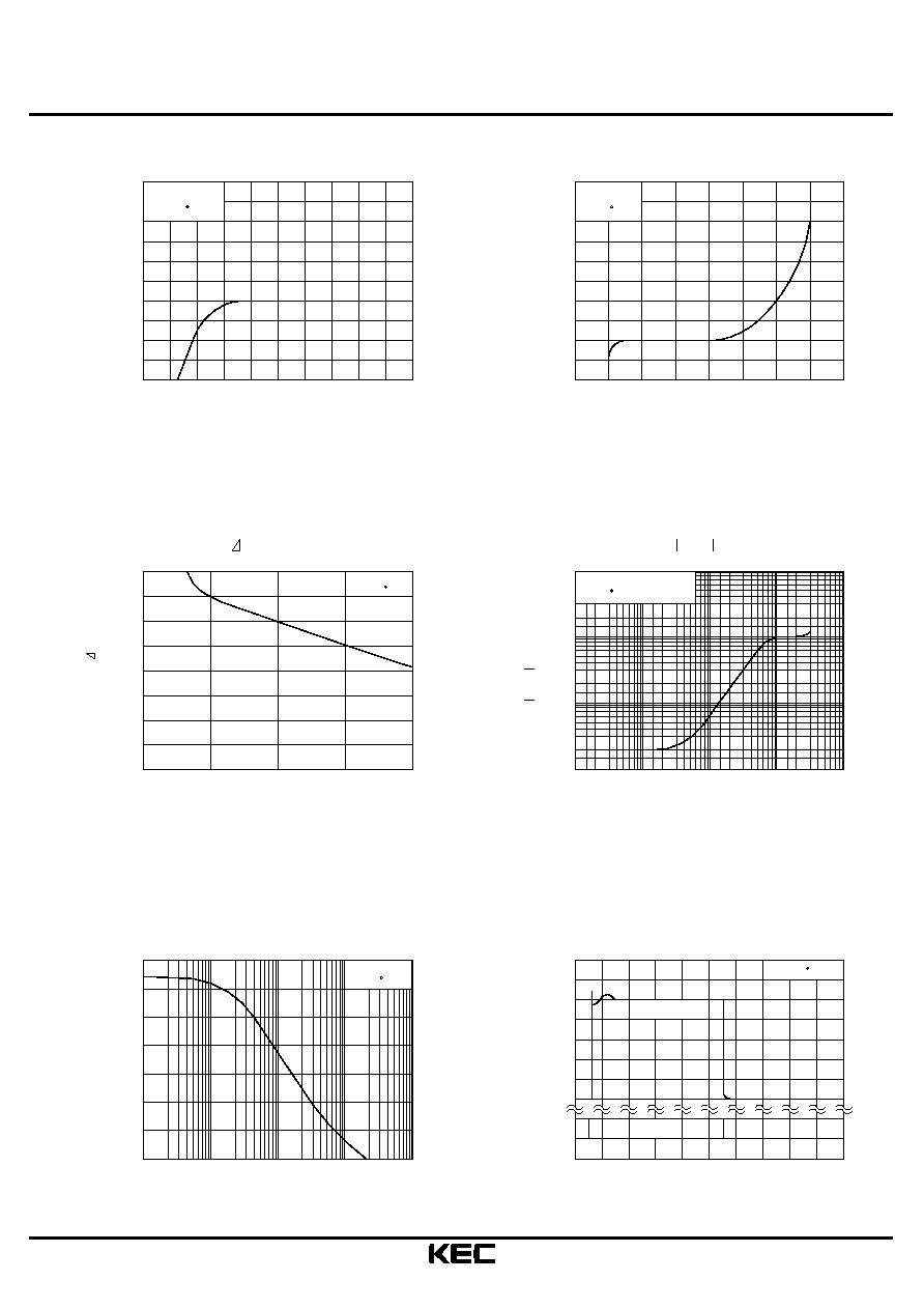
-2.0
K
I - V
CATHODE VOLTAGE V (V)
-1.0
3.0
0
1.0
2.0
-100
50
-50
CATHODE CURRENT I (mA)
0
KA
K
KA
100
150
20
10
0
5
CATHODE VOLTAGE V (V)
V - V
ref
1.0M
100k
10k
10M
1.0k
FREQUENCY f (Hz)
Zka - f
FREQUENCY f (Hz)
G - f
VO
3.0
5.0
0
VOLTAGE SWING (V)
16
12
8.0
20
4.0
TIME t (
�
s)
0
PULSE RESPONSE
-24
CHANGE IN REFERENCE INPUT
-32
-16
0
-8.0
VOLTAGE V (mV)
Zka (
)
100
10
0.1
DYNAMIC IMPEDANCE
1.0
G (dB)
0
-10
OPEN LOOP VOLTAGE GAIN
10
800
600
KA
K
KA
0
CATHODE CURRENT I (
�
A)
-200
2.0
1.0
0
3.0
-1.0
CATHODE VOLTAGE V (V)
I - V
K
200
400
V =V
Ta=25 C
KA
ref
ref
KA
Ta=25 C
V =V
ref
15
Ta=25 C
K
I =10mA
I =1.0mA~100mA
Ta=25 C
K
VO
20
30
40
50
60
1.0k
10M
10k
100k
1.0M
I =10mA
Ta=25 C
K
0
2.0
1.0
Ta=25 C
OUTPUT
INPUT
KA
KA

2005. 10. 26
5/5
KIA431S/AS/BS
Revision No : 1
ALLOWABLE POWER DISSIPATION P (mW)
D
D
P - Ta
120
80
40
0
AMBIENT TEMPERATURE Ta ( C)
0.2
0
160
0.8
1.0
THERMAL RESISTANCE
J-C
139
J-A
357
C/W
0.4
0.6
100
60
20
140