/home/web/doc/html/kingbright/176217

PHOTOCOUPLER
KB815
SPEC NO: DSAD1541
REV NO: V.1
DATE:APR/26/2003
PAGE: 1 OF 8
APPROVED: J.Lu
CHECKED:Tracy Deng
DRAWN:D.L.HUANG
FEATURES
2.High isolation voltage between input and output (Viso=5000 Vrms)
3.Compact dual-in-line package
DESCRIPTION
2.The lead pitch is 2.54mm
APPLICATIONS
1.Computer terminals
KB815:1-channel type
2.Registers, copiers, automatic vending machines
3.System appliances, measuring instruments
4.Industial robots
GaAs light emitting diode and a darlington silicon phototransistor.
GENERAL PURPOSE
HIGH ISOLATION VOLTAGE
HIGH SENSITIVITY
PHOTOCOUPLER SERIES
5.Signal transmission between circuits of different potentials and impedances
1.High current transfer ratio. (CTR:MIN.600 % at I
F
=1mA.V
CE
=2V)
4. Recognized by UL and CUL, file NO. E225308
1.The KB815 is optically coupled isolators containing a
PHOTOCOUPLER
KB815
SPEC NO: DSAD1541
REV NO: V.1
DATE:APR/26/2003
PAGE: 2 OF 8
APPROVED: J.Lu
CHECKED:Tracy Deng
DRAWN:D.L.HUANG
0.9 [0.035] 0.2
1.2 [0.047] 0.3
2
.
7
[
0
.
106]
0.5 [0.02] 0.1
7
[0
.
2
7
6
]
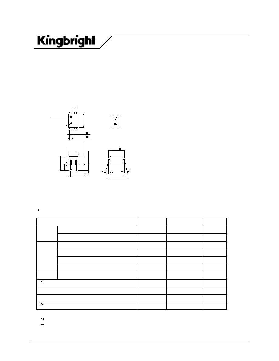
1. Anode
3
[0
.
1
1
8
]
4.58 [0.18]
3
.
5
[
0
.
138]
0
.
4
[0
.
0
1
5
]M
IN.
2
1
?= 0 to 13
Emitter
3.
Collector
4.
0.25 [0.01] 0.1
?
?
:
7.62 [0.3] 0.3
* PACKAGE DIMENSIONS (UNIT: mm)
DIP Type
6
.
5
[
0
.
256]
KB8
1
5
3
4
Top View
2.54 [0.1] 0.25
KB815
TOLERANCE : �0.5[�0.02] UNLESS OTHERWISE NOTED.
Internal connection
diagram
CTR
rank mark
mark
Anode
2. Cathode
2
1
3
4
mA
I
F
Forward current
Power dissipation
Collector-emitter voltage
Collector current
Collector power dissipation
Total power dissipation
Emitter-collector voltage
Operating temperature
Storage temperature
Soldering temperature
For 10 seconds
40 to 60%RH, AC for 1 minute
Isolation voltage
Output
Input
:C
-55~+125
Tstg
260
Tsol
:C
mA
80
I
C
-30~+100
5000
Topr
Viso
:C
V
rms
200
150
P
C
Ptot
mW
mW
V
ECO
V
CEO
6
V
35
V
P
70
mW
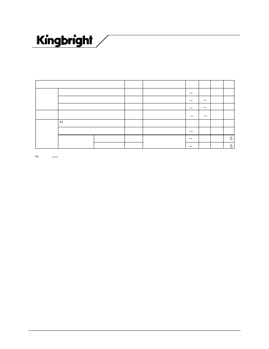
Absolute Maximum Ratings
Symbol
Parameter
(Ta=25:)
Rating
Unit
50
C
PHOTOCOUPLER
KB815
SPEC NO: DSAD1541
REV NO: V.1
DATE:APR/26/2003
PAGE: 3 OF 8
APPROVED: J.Lu
CHECKED:Tracy Deng
DRAWN:D.L.HUANG
Transfer
charact-
eristics
Response time
Rise time
Fall time
t
V
CE
=2V, I
C
=10mA,R
L
=100
[
53
250
60
300
C
C
Forward voltage
* Electro-optical Characteristics
Current transfer ratio
Peak forward voltage
Collector dark current
Collector-emitter saturation voltage
Input
Output
I
FM
=0.5A
3.0
V
FM
V
CE(
sat
)
CTR
I
CEO
I
F
=20mA, I
C
=5mA
I
F
=1mA, V
CE
=2V
0.8
1.0
600
7500
V
CE
=10V,I
F
=0mA
-6
10
Parameter
V
F
Symbol
I
F
=20mA
Conditions
1.2
1.4
Typ.
Min.
Max.
V
V
%
A
V
Unit
t
f
r
X 100%
CTR= Ic
F
I
1600
Reverse current
I
R
V
R
=4V
10
uA
PHOTOCOUPLER
KB815
SPEC NO: DSAD1541
REV NO: V.1
DATE:APR/26/2003
PAGE: 4 OF 8
APPROVED: J.Lu
CHECKED:Tracy Deng
DRAWN:D.L.HUANG
10
C
o
lle
c
t
o
r
d
a
r
k
c
u
r
r
e
n
t
I
CE
O
(A
)
-25
25
0
10
-9
100
75
50
-7
10
-8
10
-6
10
-5
V
+-
=10V
10
-4
50
F
o
r
w
ar
d
c
u
r
r
e
n
t
I
F
(m
A
)
2.0
1
0.5
0
1.5
1.0
2
3.5
2.5 3.0
5
20
200
100
500
-10
10
-25
Rel
a
t
i
o
v
ecurr
ent t
ra
n
s
f
e
r
r
a
t
i
o
n
(
%)
50
0
100
150
0
25
75
50
100
50
0.8
0.9
0.7
0.6
0.5
0.4
0.3
0.1
0.2
-25
0
0
25
1.0
100
75
C
I
.
=10mA
40
C
o
l
l
e
c
t
o
r
c
urr
ent
I
C
(m
A
)
0
0
2
1
3
20
80
60
100
1mA
5
4
2mA
5mA
Pc(MAX)
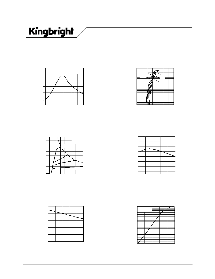
Fig. 1 Current Transfor Ratio vs.
Forward Current
Fig. 2 Forward Current vs.
Forward voltage
Fig. 4 Relative Current Transfer Ratio
vs. Ambient Temperature
Fig. 3 Collector Current vs.
Collector-emitter Voltage
Fig. 5 Collector-emitter Saturation
Voltage vs. Ambient Temperature
Fig. 6 Collector Dark Current vs.
Ambient Temperature
Ta=75:C
50:C
25:
C
0:C
-25:C
10
Ta=25 :
C
Ambient temperature Ta (:C)
400
800
1200
1600
2000
2400
0
0.1 0.2 0.5
1
2 3 4 5 6 7
10
Cur
r
en
t
t
r
ansfer
r
a
t
i
o
C
T
R
(
%)
V
+-
=2V
Ta=25:C
I
.
=1mA
V
+-
=2V
C
o
l
l
e
c
t
o
r
-
e
m
i
t
t
er
s
at
urat
i
o
n
v
o
l
t
a
g
e
V
CE
(sat)
(
V
)
I =20mA
I =5mA
.
+
Ambient temperature Ta(:C)
Collector-emitter voltage V
+-
(V)
Forward current I
.
(mA)
Forward voltage V
.
8
Ambient temperature
Ta(:)
PHOTOCOUPLER
KB815
SPEC NO: DSAD1541
REV NO: V.1
DATE:APR/26/2003
PAGE: 5 OF 8
APPROVED: J.Lu
CHECKED:Tracy Deng
DRAWN:D.L.HUANG
10
Re
sp
o
n
se
ti
me
(
0.05
0.1
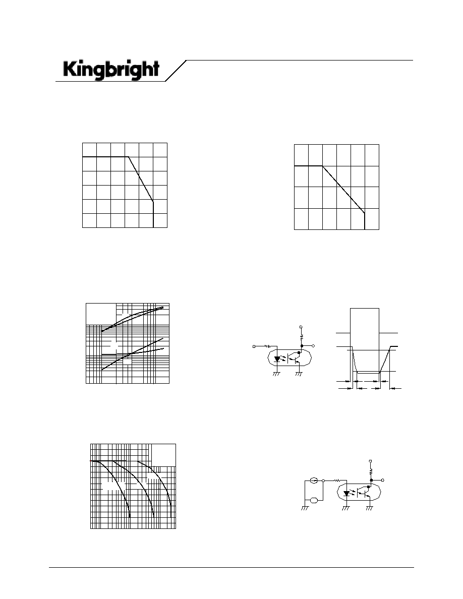
Fig. 10 Frequency Response
Load resistance R
V
o
l
t
age
g
a
i
n
A
v
(
dB
)
-20
-10
0
1
0.05
5
t
d
D
Test Circuit for Frequency Response
R
Frequency f(kHz)
1
0.5
0.2
5
2
50
100
[
R
L
=10K
[
1k
[
s
CE
=2mA
Ta=25
V
I
C
=2V
:C
0.5
0.2
1
(K[)
L
d
t
2
t
Output
R
L
Vcc
90%
r
f
t
s
t
=2V
=10mA
Ta=25
Fig. 9 Response Time vs.
Load Resistance
Fig. 7 Forward Current vs.
Ambient Temperature
Ambient temperature Ta( C)
100
s)
g
50
500
200
V
CE
I
C
F
o
rward
curr
ent I
F
(m
A)
-25
0
10
0
20
30
40
50
60
Ambient Temperature
Output
Input
Ambient temperature Ta(
Test Circuit for Response Time
Co
lle
cto
r
p
o
w
e
r
d
i
s
si
p
a
tio
n
P
c(mW
)
-25
0
25
50
t d
tr
:C
tf
:
Input R
D
Output
R
L
Vcc
25
50
75
100
125
100
50
0
150
200
75
100
125
10%
:
C)
Fig. 8 Collector Power Dissipation vs.