
LG Semicon Co.,Ltd.
REVISION HISTORY
/ Revision 1.0: July 1998
- Add PC100,7K(2-2-2) Specifications.
- Update Icc Specifications.
- Change Input Test Condition from 2.8/0.0V to 2.4/0.4V.
- Added post SPD Information separately(7K/7J/10K) for Modules.
- Add Minimum Capacitance Value for Component.
Rev. 1.0
GM72V66841CT/CLT
2,097,152 WORD x 8 BIT x 4 BANK
SYNCHRONOUS DYNAMIC RAM
Description
The GM72V66841CT/CLT is a synchronous
dynamic random access memory comprised of
67,108,864 memory cells and logic including
input and output circuits operating synchronously
by referring to the positive edge of the externally
provided Clock.
The GM72V66841CT/CLT provides four
banks of 2,097,152 word by 8 bit to realize high
bandwidth with the Clock frequency up to 125
Mhz.
Features
* PC100,PC66 Compatible
7K(2-2-2), 7J(3-2-2), 10K(PC66)
* 3.3V single Power supply
* LVTTL interface
* Max Clock frequency
100/125 MHz
* 4,096 refresh cycle per 64 ms
* Two kinds of refresh operation
Auto refresh/ Self refresh
* Programmable burst access capability ;
- Sequence:Sequential / Interleave
- Length :1/2/4/8/FP
* Programmable CAS latency : 2/3
* 4 Banks can operate independently or
simultaneously
* Burst read/burst write or burst read/single
write operation capability
* Input and output masking by DQM input
* One Clock of back to back read or write
command interval
* Synchronous Power down and Clock
suspend capability with one Clock latency
for both entry and exit
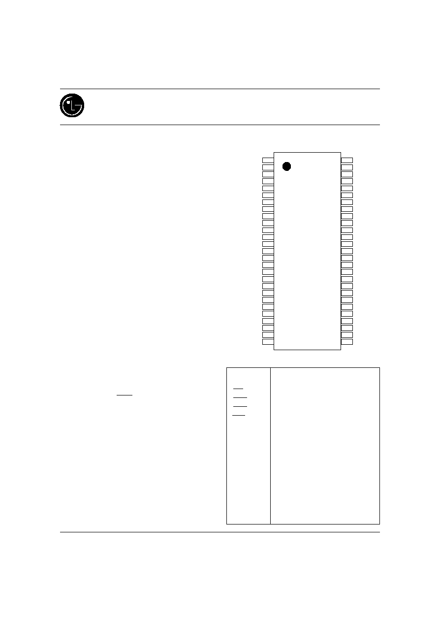
*JEDEC Standard 54Pin 400mil TSOP II
Package
Pin Configuration
LG Semicon Co.,Ltd.
Pin Name
CLK
CKE
CS
RAS
CAS
WE
A0~A9,A11
A10 / AP
BA0/A13
~BA1/A12
DQ0~DQ7
DQM
VCCQ
VSSQ
VCC
VSS
NC
Clock
Clock Enable
Chip Select
Row Address Strobe
Column Address Strobe
Write Enable
Address input
Address input or Auto Precharge
Bank select
Data input / Data output
Data input / output Mask
V
CC
for DQ
V
SS
for DQ
Power for internal circuit
Ground for internal circuit
No Connection
1
2
3
4
5
6
7
8
9
10
11
12
13
14
15
16
17
18
19
20
21
22
23
24
25
26
27
JEDEC STANDARD
400 mil 54 PIN TSOP II
(TOP VIEW)
54
53
52
51
50
49
48
47
46
45
44
43
42
41
40
39
38
37
36
35
34
33
32
31
30
29
28
VCC
DQ0
VCCQ
NC
DQ1
VSSQ
NC
DQ2
VCCQ
NC
DQ3
VSSQ
NC
VCC
NC
/WE
/CAS
/RAS
/CS
BA0/A13
BA1/A12
A10,AP
A0
A1
A2
A3
VCC
VSS
DQ7
VSSQ
NC
DQ6
VCCQ
NC
DQ5
VSSQ
NC
DQ4
VCCQ
NC
VSS
NC
DQM
CLK
CKE
NC
A11
A9
A8
A7
A6
A5
A4
VSS
1

LG Semicon
GM72V66841CT/CLT
2
Block Diagram
A0 to A13
A0 to A8
A0 to A13
Column address
counter
Column address
buffer
Row address
counter
Refresh
counter
Input
buffer
Output
buffer
DQ0 to DQ7
Control logic &
timing generator
CLK
CKE
DQM
RAS
CAS
Row decoder
Memory array
Bank 0
4096 row
x 512 column
x 8 bit
Column decoder
Sense amplifier & I/O bus
Row decoder
Memory array
Bank 1
4096 row
x 512 column
x 8 bit
Column decoder
Sense amplifier & I/O bus
Row decoder
Memory array
Bank 2
4096 row
x 512 column
x 8 bit
Column decoder
Sense amplifier & I/O bus
Row decoder
Memory array
Bank 3
4096 row
x 512 column
x 8 bit
Column decoder
Sense amplifier & I/O bus
CS
WE
LG Semicon
GM72V66841CT/CLT
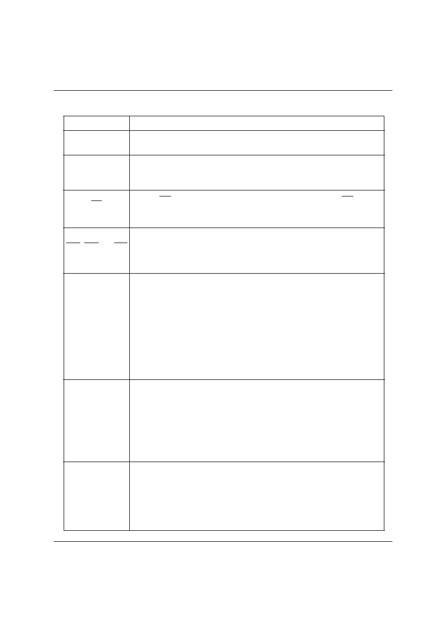
Pin Description
Pin Name
DESCRIPTION
CLK
(input pin)
CLK is the master Clock input to this pin. The other input signals are referred
at CLK rising edge.
CKE
(input pin)
This pin determines whether or not the next CLK is valid. If CKE is High, the
next CLK rising edge is valid. If CKE is Low, the next CLK rising edge is
invalid. This pin is used for Power-down and Clock suspend modes.
CS
(input pin)
When CS is Low, the command input cycle becomes valid. When CS is high,
all inputs are ignored. However, internal operations (bank active, burst
operations, etc.) are held.
Although these pin names are the same as those of conventional DRAMs,
they function in a different way. These pins define operation commands (read,
write, etc.) depending on the combination of their voltage levels. For details,
refer to the command operation section.
RAS, CAS, and WE
(input pins)
A0 ~ A11
(input pins)
Row address (AX0 to AX11) is determined by A0 to A11 level at the bank
active command cycle CLK rising edge. Column address(AY0 to AY8;
GM72V66841CT/CLT) is determined by A0 to A8 level at the read or write
command cycle CLK rising edge. And this column address becomes burst
access start address. A10 defines the Precharge mode. When A10 = High at
the Precharge command cycle, all banks are Precharged. But when A10 =
Low at the Precharge command cycle, only the bank that is selected by
A12/A13 (BS) is Precharged.
A12/A13
(input pin)
A12/A13 are bank select signal (BS). The memory array of the
GM72V66841CT/CLT is divided into bank 0, bank 1, bank2 and bank 3.
GM72V66841CT/CLT contain 4096-row x 512-column x 8-bits. If A12 is
Low and if A13 is Low, bank 0 is selected. If A12 is High and A13 is Low,
bank 1 is selected. If A12 is Low and A13 is High, bank 2 is selected. If A12
is High and A13 is High, bank 3 is selected.
DQM,
DQMU/DQML
(input pins)
DQM, DQMU/DQML controls input/output buffers.
* Read operation: If DQM, DQMU/DQML is High, The output buffer
becomes High-Z. If the DQM, DQMU/DQML is Low, the output buffer
becomes Low-Z.
* Write operation: If DQM, DQMU/DQML is High, the previous data is held
(the new data is not written). If DQM, DQMU/DQML is Low, the data is
written.
3
LG Semicon
GM72V66841CT/CLT
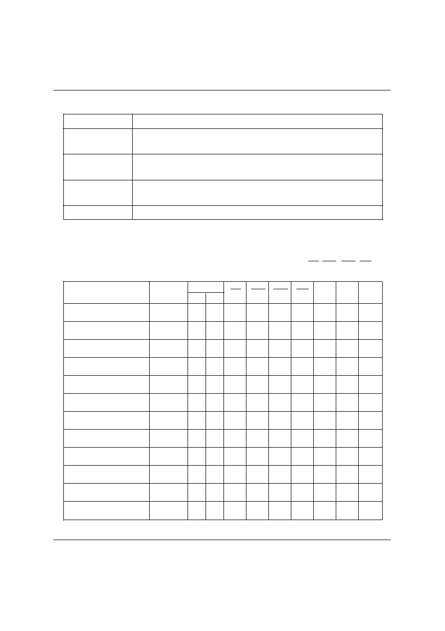
Command Operation
Command Truth Table
* Notes : H: V
IH
, L: V
IL
, X: V
IH
or V
IL
, V: Valid address input
The synchronous DRAM recognizes the following commands specified by the CS, RAS, CAS, WE
and address pins.
Function
Ignore command
Symbol
CKE
No Operation
Burst stop in full page
Column address and
read command
Read with auto-Precharge
Write with auto-Precharge
Row address strobe and
bank active
Precharge all banks
Column address and
write command
CS
RAS
CAS
WE
A12~
A13
A10
A0~
A11
DESL
NOP
BST
READ
READ A
WRIT
WRIT A
ACTV
PALL
H
H
H
H
H
H
H
H
H
H
X
X
X
X
X
X
X
X
X
V
H
L
L
L
L
L
L
L
L
L
X
H
H
H
H
H
H
L
L
L
X
H
H
L
L
L
L
H
H
L
X
H
L
H
H
L
L
H
L
H
X
X
X
V
V
V
V
V
X
X
X
X
X
L
H
L
H
V
H
X
X
X
X
V
V
V
V
V
X
X
n-1
n
H
X
L
L
L
L
V
V
V
Mode register set
MRS
Refresh
REF/SELF
Precharge select bank
PRE
H
X
L
L
H
L
V
L
X
4
V
SS
and V
SSQ
(Power supply pins)
Ground is connected. (V
SS
is for the internal circuit and V
SSQ
is for the output
buffer.)
NC
No Connection pins.
DESCRIPTION
Pin Name
V
CC
and V
CCQ
(Power supply pins)
3.3 V is applied. (V
CC
is for the internal circuit and V
CCQ
is for the output
buffer.)
DQ0 ~ DQ7
(I/O pins)
Data is input and output from these pins. These pins are the same as those of a
conventional DRAM.
Pin Description(Continued)