 | –≠–ª–µ–∫—Ç—Ä–æ–Ω–Ω—ã–π –∫–æ–º–ø–æ–Ω–µ–Ω—Ç: DCR1474SV | –°–∫–∞—á–∞—Ç—å:  PDF PDF  ZIP ZIP |
1/10
www.dynexsemi.com
DCR1474SY / DCR1474SV
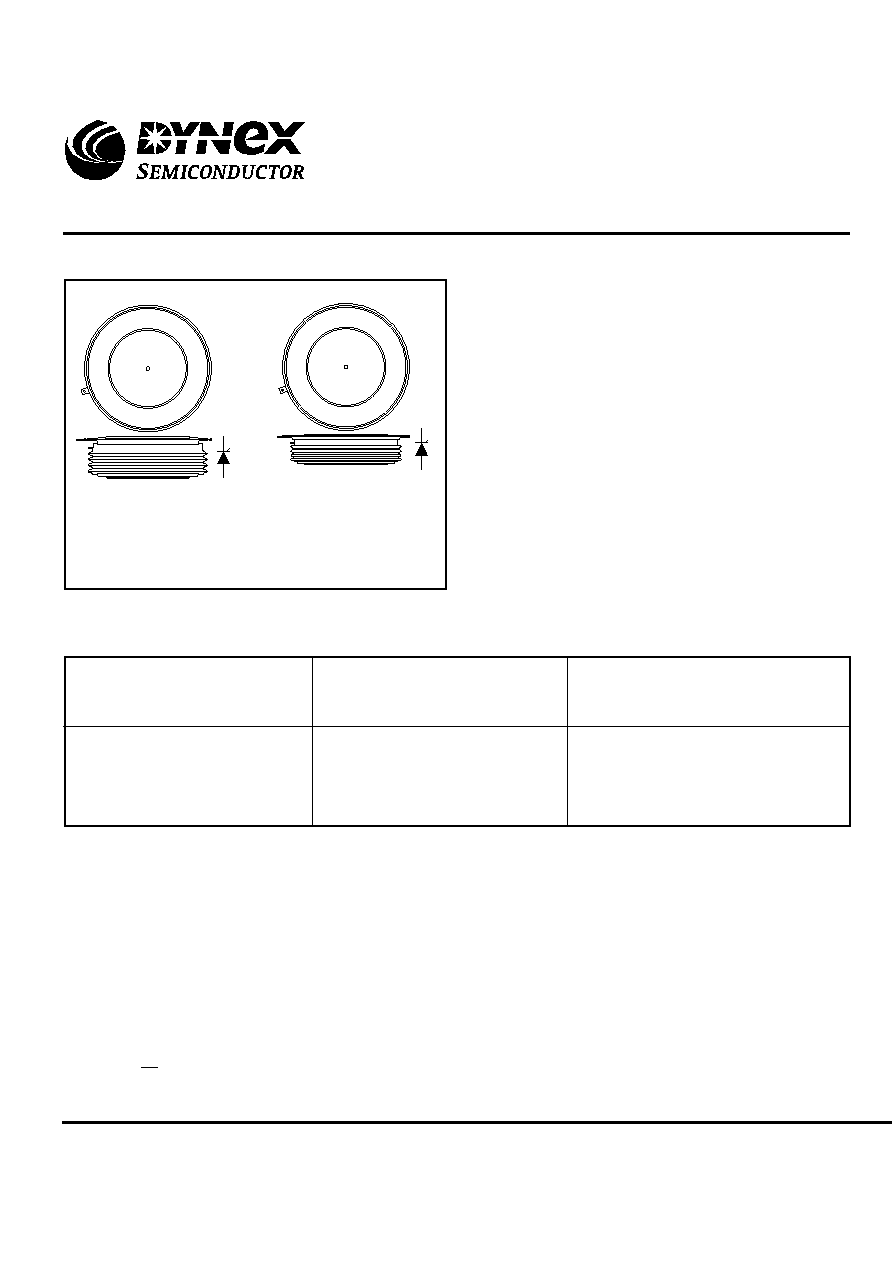
PACKAGE OUTLINE
KEY PARAMETERS
V
DRM
1800V
I
T(AV)
3600A
I
TSM
61200A
dVdt*
1000V/
µ
s
dI/dt
300A/
µ
s
*Higher dV/dt selections available
DCR1474SY / DCR1474SV
Phase Control Thyristor
Advance Information
Replaces July 2001 version, DS4649-6.0
DS4649-7.3 November 2002
See Package Details for further information.
Fig. 1 Package outline
Outline type code: Y
Outline type code: V
VOLTAGE RATINGS
ORDERING INFORMATION
When ordering, select the required part number shown in the
Voltage Ratings selection table.
For example:
DCR1474SY18 for an 1800V 'Y' outline variant
or
DCR1474SV18 for an 1800V 'V' outline variant
If a lower voltage grade is required, then use V
DRM
/100 for the
grade required e.g.:
DCR1474SY16 for a 1600V 'Y' outline variant etc.
Note: Please use the complete part number when ordering and quote
this number in any future correspondance relating to your order.
DCR1474SY18
or
DCR1474SV18
Conditions
T
vj
= 0∞ to 125∞C.
I
DRM
= I
RRM
= 250mA.
V
DRM
, V
RRM
= 10ms 1/2 sine.
V
DSM
& V
RSM
= V
DRM
& V
RRM
+ 100V
respectively.
Lower voltage grades available.
Part Number
Repetitive Peak Voltages
V
DRM
V
RRM
V
1800
1800

2/10
www.dynexsemi.com
DCR1474SY / DCR1474SV
CURRENT RATING
T
case
= 80∞C unless stated otherwise.
Symbol
Parameter
Conditions
Double Side Cooled
I
T(AV)
Mean on-state current
I
T(RMS)
RMS value
I
T
Continuous (direct) on-state current
Single Side Cooled (Anode side)
I
T(AV)
Mean on-state current
I
T(RMS)
RMS value
I
T
Continuous (direct) on-state current
Units
Max.
Half wave resistive load
2785
A
-
4370
A
-
3750
A
Half wave resistive load
1750
A
-
2745
A
-
2170
A
CURRENT RATING
T
case
= 60∞C unless stated otherwise.
Symbol
Parameter
Conditions
Double Side Cooled
I
T(AV)
Mean on-state current
I
T(RMS)
RMS value
I
T
Continuous (direct) on-state current
Single Side Cooled (Anode side)
I
T(AV)
Mean on-state current
I
T(RMS)
RMS value
I
T
Continuous (direct) on-state current
Units
Max.
Half wave resistive load
3600
A
-
5655
A
-
4996
A
Half wave resistive load
2279
A
-
3580
A
-
2897
A

3/10
www.dynexsemi.com
DCR1474SY / DCR1474SV
SURGE RATINGS
Conditions
10ms half sine; T
case
= 125
o
C
V
R
= 50% V
RRM
- 1/4 sine
10ms half sine; T
case
= 125
o
C
V
R
= 0
Max.
Units
Symbol
Parameter
I
TSM
Surge (non-repetitive) on-state current
I
2
t
I
2
t for fusing
I
TSM
Surge (non-repetitive) on-state current
I
2
t
I
2
t for fusing
18.75 x 10
6
A
2
s
61.2
kA
12.0 x 10
6
A
2
s
49.0
kA
THERMAL AND MECHANICAL DATA
dc
Conditions
Min.
Max.
Units
o
C/W
-
0.019
Anode dc
Clamping force 43kN
with mounting compound
Thermal resistance - case to heatsink
R
th(c-h)
0.002
Double side
-
125
o
C
T
vj
Virtual junction temperature
T
stg
Storage temperature range
Reverse (blocking)
Single side
-
Thermal resistance - junction to case
R
th(j-c)
Single side cooled
Symbol
Parameter
Clamping force
38
47
kN
≠55
125
o
C
-
On-state (conducting)
-
135
o
C
-
0.004
o
C/W
o
C/W
Cathode dc
-
0.019
o
C/W
Double side cooled
-
0.0095
o
C/W
4/10
www.dynexsemi.com
DCR1474SY / DCR1474SV
DYNAMIC CHARACTERISTICS
Parameter
Symbol
Conditions
Max.
Units
GATE TRIGGER CHARACTERISTICS AND RATINGS
V
DRM
= 5V, T
case
= 25
o
C
Conditions
Parameter
Symbol
V
GT
Gate trigger voltage
V
DRM
= 5V, T
case
= 25
o
C
I
GT
Gate trigger current
V
GD
Gate non-trigger voltage
At V
DRM
T
case
= 125
o
C
4.0
V
400
mA
0.25
V
Max.
Units
I
RRM
/I
DRM
Peak reverse and off-state current
At V
RRM
/V
DRM
, T
case
= 125
o
C
From 67% V
DRM
to 1000A
Gate source 20V, 10
t
r
0.5
µ
s to 1A, T
j
= 125
o
C
dV/dt
Maximum linear rate of rise of off-state voltage
To 67% V
DRM
T
j
= 125
o
C.
250
mA
1000
V/
µ
s
Repetitive 50Hz
150
A/
µ
s
Non-repetitive
300
A/
µ
s
Rate of rise of on-state current
dI/dt
V
T(TO)
Threshold voltage
At T
vj
= 125
o
C
r
T
On-state slope resistance
At T
vj
= 125
o
C
t
gd
Delay time
0.92
V
0.09
m
2
µ
s
V
D
= 67% V
DRM
, Gate source 30V, 15
t
r
0.5
µ
s, T
j
= 25
o
C
I
T
= 1000A, t
p
= 1ms, T
j
= 125∞C,
V
R
= 50V, dI
RR
/dt = 20A/
µ
s,
V
DR
= 67% V
DRM
, dV
DR
/dt = 20V/
µ
s linear
µ
s
200
Turn-off time
t
q
I
L
Latching current
T
j
= 25
o
C, V
D
= 5V
I
H
Holding current
T
j
= 25
o
C, R
g-k
=
1000
mA
300
mA
V
FGM
Peak forward gate voltage
Anode positive with respect to cathode
V
FGN
Peak forward gate voltage
Anode negative with respect to cathode
V
RGM
Peak reverse gate voltage
I
FGM
Peak forward gate current
Anode positive with respect to cathode
P
GM
Peak gate power
See table, gate characteristics curve
P
G(AV)
Mean gate power
30
V
0.25
V
5
V
30
A
150
W
10
W

5/10
www.dynexsemi.com
DCR1474SY / DCR1474SV
CURVES
Fig.2 Maximum (limit) on-state characteristics
V
TM
Equation:-
V
TM
= A + Bln (I
T
) + C.I
T
+D.
I
T
Where
A = 0.7635305
B = 8.73036 x 10
≠3
C = 8.568357 x 10
≠5
D = 1.537158 x 10
≠3
These values are valid for T
j
= 125∞C for I
T
500A to 10000A
0.5
1.0
1.5
2.0
Instantaneous on-state voltage, V
T
- (V)
0
2000
4000
6000
8000
10000
Instantaneous on-state current, I
T
- (A)
Measured under pulse conditions
T
j
= 125∞C
Fig.3 Gate characteristics
10
1
0.1
0.01
0.001
Gate trigger current, I
GT
- (A)
100
10
1
0.1
Gate trigger voltage, V
GT
- (V)
100W
50W
20W
10W
5W
2W
T
j
= 125
∞
C
T
j
= 25
∞
C
T
j
= -40
∞
C
Upper limit 99%
Lower
limit
1%
Pulse width
µs
100
200
500
1ms
10ms
50
150
150
150
150
20
100
150
150
150
100
-
400
150
125
100
25
-
Pulse frequency Hz
Table gives pulse power P
GM
in Watts