 | –≠–ª–µ–∫—Ç—Ä–æ–Ω–Ω—ã–π –∫–æ–º–ø–æ–Ω–µ–Ω—Ç: 2847 | –°–∫–∞—á–∞—Ç—å:  PDF PDF  ZIP ZIP |

1
LTC2847
sn2847 2847fs
APPLICATIO S
U
DESCRIPTIO
U
FEATURES
TYPICAL APPLICATIO
U
, LTC and LT are registered trademarks of Linear Technology Corporation.
Complete DTE or DCE Multiprotocol Serial Interface with DB-25 Connector
s
Data Networking
s
CSU and DSU
s
Data Routers
s
Software-Selectable Transceiver Supports:
RS232, RS449, EIA530, EIA530-A, V.35, V.36, X.21
s
Operates from Single 5V Supply
s
Separate Supply Pin for Digital Interface Works
down to 3V
s
On-Chip Cable Termination
s
Complete DTE or DCE Port with LTC2845
s
Available in 38-Pin 5mm
◊
7mm QFN Package
The LTC
Æ
2847 is a 3-driver/3-receiver multiprotocol trans-
ceiver with on-chip cable termination. When combined with
the LTC2845, this chip set forms a complete software-
selectable DTE or DCE interface port that supports the
RS232, RS449, EIA530, EIA530-A, V.35, V.36 and X.21
protocols. All necessary cable termination is provided inside
the LTC2847.
The V
CC
supplies the drivers, the receivers and an internal
charge pump that requires only five space-saving surface
mounted capacitors. The V
IN
supply drives the digital inter-
face circuitry including the receiver output drivers. It can be
tied to V
CC
or be powered off a lower supply (down to 3V) to
interface with low voltage ASICs. The LTC2847 is available in
a 0.8mm tall, 5mm
◊
7mm QFN package.
Software-Selectable
Multiprotocol Transceiver with
Termination and 3.3V Digital Interface
D2
D1
LTC2845
RTS
DTR
DSR
DCD
CTS
D3
R2
R1
R4
R3
LTC2847
RI
LL
TM
RL
TXD
SCTE
TXC
RXC
RXD
2
14
24
11
15
12
17
9
3
1
4
19
20
8
23
10
5
13
6
22
18
25
21
7
16
2847 TA01
D1
SCTE B
SCTE A (113)
TXD B
TXD A (103)
RXC A (115)
RXC B
RXD A (104)
RXD B
RTS A (105)
RTS B
DTR A (108)
DTR B
LL A (141)
TM (142)
RL (140)
SG (102)
SHIELD (101)
DB-25 CONNECTOR
TXC A (114)
DCD A (109)
DCD B
DSR A (107)
DSR B
D4
R5
D5
D2
D3
R1
R2
R3
TXC B
T
T
T
T
T
CTS A (106)
CTS B
RI (125)
*
*OPTIONAL

2
LTC2847
sn2847 2847fs
ORDER PART
NUMBER
(Note 1)
V
CC
Voltage .............................................. ≠ 0.3V to 6.5V
V
IN
Voltage .............................................. ≠ 0.3V to 6.5V
Input Voltage
Transmitters ........................... ≠ 0.3V to (V
CC
+ 0.3V)
Receivers ............................................... ≠ 18V to 18V
Logic Pins .............................. ≠ 0.3V to (V
CC
+ 0.3V)
Output Voltage
Transmitters ................. (V
EE
≠ 0.3V) to (V
DD
+ 0.3V)
Receivers ................................. ≠ 0.3V to (V
IN
+ 0.3V)
V
EE
........................................................ ≠ 10V to 0.3V
V
DD
....................................................... ≠ 0.3V to 10V
Short-Circuit Duration
Transmitter Output ..................................... Indefinite
Receiver Output .......................................... Indefinite
V
EE
.................................................................. 30 sec
Operating Temperature Range
LTC2847C ............................................... 0
∞
C to 70
∞
C
LTC2847I ........................................... ≠ 40
∞
C to 85
∞
C
Storage Temperature Range ................ ≠ 65
∞
C to 150
∞
C
Lead Temperature (Soldering, 10 sec)................. 300
∞
C
LTC2847CUHF
LTC2847IUHF
ABSOLUTE AXI U RATI GS
W
W
W
U
PACKAGE/ORDER I FOR ATIO
U
U
W
The
q
denotes specifications which apply over the full operating
temperature range, otherwise specifications are at T
A
= 25
∞
C. V
CC
= 5V, V
IN
= 3.3V, unless otherwise noted (Notes 2, 3)
ELECTRICAL CHARACTERISTICS
Consult LTC Marketing for parts specified with wider operating temperature ranges.
UHF PART
MARKING
2847
2847I
13 14 15 16
TOP VIEW
UHF PACKAGE
38-LEAD (7mm
◊
5mm) PLASTIC QFN
UNDERSIDE METAL INTERNALLY CONNECTED TO V
EE
(PCB CONNECTION OPTIONAL)
17 18 19
38 37 36 35 34 33 32
24
25
26
27
28
29
30
31
8
7
6
5
4
3
2
1
23
22
21
20
9
10
11
12
NC
V
DD
NC
V
CC
D1
D2
D3
R1
R2
R3
M0
M1
V
IN
M2
DCE/DTE
R3 B
R3 A
NC
NC
C1
+
C1
≠
V
EE
C2
+
C2
≠
V
EE
V
EE
GND
GND
D1 A
D1 B
D2 A
D2 B
D3/R1 A
D3/R1 B
NC
NC
R2 A
R2 B
T
JMAX
= 125
∞
C,
JA
= 34
∞
C/W
SYMBOL
PARAMETER
CONDITIONS
MIN
TYP
MAX
UNITS
Supplies
I
CC
V
CC
Supply Current (DCE Mode,
RS530, RS530-A, X.21 Modes, No Load
14
mA
All Digital Pins = GND or V
IN
)
RS530, RS530-A, X.21 Modes, Full Load
q
100
130
mA
V.35 Mode
q
126
170
mA
V.28 Mode, No Load
20
mA
V.28 Mode, Full Load
q
35
75
mA
No-Cable Mode
q
300
900
µ
A
I
VIN
V
IN
Supply Current
All Modes Except No-Cable Mode
405
µ
A
(DCE Mode, All Digital Pins = GND or V
IN
)
P
D
Internal Power Dissipation (DCE Mode)
RS530, RS530-A, X.21 Modes, Full Load
410
mW
V.35 Mode, Full Load
625
mW
V.28 Mode, Full Load
150
mW
V
+
Positive Charge Pump Output Voltage
V.11 or V.28 Mode, No Load
q
8
9.3
V
V.35 Mode
q
7
8.0
V
V.28 Mode, with Load
q
8
8.7
V
V.28 Mode, with Load, I
DD
= 10mA
6.5
V

3
LTC2847
sn2847 2847fs
The
q
denotes specifications which apply over the full operating
temperature range, otherwise specifications are at T
A
= 25
∞
C. V
CC
= 5V, V
IN
= 3.3V, unless otherwise noted (Notes 2, 3)
ELECTRICAL CHARACTERISTICS
SYMBOL
PARAMETER
CONDITIONS
MIN
TYP
MAX
UNITS
V
≠
Negative Charge Pump Output Voltage
V.28 Mode, No Load
≠ 9.6
V
V.28 Mode, Full Load
q
≠ 7.5
≠ 8.5
V
V.35 Mode
q
≠ 5.5
≠ 6.5
V
RS530, RS530-A, X.21 Modes, Full Load
q
≠ 4.5
≠ 6.0
V
f
OSC
Charge Pump Oscillator Frequency
500
kHz
t
r
Charge Pump Rise Time
No-Cable Mode/Power-Off to Normal Operation
2
ms
Logic Inputs and Outputs
V
IH
Logic Input High Voltage
D1, D2, D3, M0, M1, M2, DCE/DTE
q
2.0
V
V
IL
Logic Input Low Voltage
D1, D2, D3, M0, M1, M2, DCE/DTE
q
0.8
V
I
IN
Logic Input Current
D1, D2, D3
q
±
10
µ
A
M0, M1, M2, DCE/DTE = GND
q
≠ 30
≠ 75
≠ 120
µ
A
M0, M1, M2, DCE/DTE = V
IN
q
±
10
µ
A
V
OH
Output High Voltage
I
O
= ≠ 3mA
q
2.7
3
V
V
OL
Output Low Voltage
I
O
= 1.6mA
q
0.2
0.4
V
I
OSR
Output Short-Circuit Current
0V
V
O
V
IN
q
±
50
mA
I
OZR
Three-State Output Current
M0 = M1 = M2 = V
IN
, V
O
= GND
q
≠30
≠85
≠160
µ
A
M0 = M1 = M2 = V
IN
, V
O
= V
IN
q
±
10
µ
A
V.11 Driver
V
ODO
Open Circuit Differential Output Voltage
R
L
= 1.95k (Figure 1)
q
±
5
V
V
ODL
Loaded Differential Output Voltage
R
L
= 50
(Figure 1)
0.5V
ODO
0.67V
ODO
V
R
L
= 50
(Figure 1)
q
±
2
V
V
OD
Change in Magnitude of Differential
R
L
= 50
(Figure 1)
q
0.2
V
Output Voltage
V
OC
Common Mode Output Voltage
R
L
= 50
(Figure 1)
q
3
V
V
OC
Change in Magnitude of Common Mode
R
L
= 50
(Figure 1)
q
0.2
V
Output Voltage
I
SS
Short-Circuit Current
V
OUT
= GND
±
150
mA
I
OZ
Output Leakage Current
V
A
and
V
B
0.25V, Power Off or
q
±
1
±
100
µ
A
No-Cable Mode or Driver Disabled
t
r
, t
f
Rise or Fall Time
(Figures 2, 13)
q
2
15
25
ns
t
PLH
Input to Output Rising
(Figures 2, 13)
q
15
40
65
ns
t
PHL
Input to Output Falling
(Figures 2, 13)
q
15
40
65
ns
t
Input to Output Difference,
t
PLH
≠ t
PHL
(Figures 2, 13)
q
0
3
12
ns
t
SKEW
Output to Output Skew
(Figures 2, 13)
3
ns

4
LTC2847
sn2847 2847fs
The
q
denotes specifications which apply over the full operating
temperature range, otherwise specifications are at T
A
= 25
∞
C. V
CC
= 5V, V
IN
= 3.3V, unless otherwise noted (Notes 2, 3)
ELECTRICAL CHARACTERISTICS
SYMBOL
PARAMETER
CONDITIONS
MIN
TYP
MAX
UNITS
V.11 Receiver
V
TH
Input Threshold Voltage
≠ 7V
V
CM
7V
q
≠ 0.2
0.2
V
V
TH
Input Hysteresis
≠ 7V
V
CM
7V
q
15
40
mV
R
IN
Input Impedance
≠7V
V
CM
7V (Figure 3)
q
100
103
t
r
, t
f
Rise or Fall Time
C
L
= 50pF (Figures 4, 14)
15
ns
t
PLH
Input to Output Rising
C
L
= 50pF (Figures 4, 14)
q
50
90
ns
t
PHL
Input to Output Falling
C
L
= 50pF (Figures 4, 14)
q
50
90
ns
t
Input to Output Difference,
t
PLH
≠ t
PHL
C
L
= 50pF (Figures 4, 14)
q
0
4
25
ns
V.35 Driver
V
OD
Differential Output Voltage
Open Circuit, R
L
= 1.95k (Figure 5)
q
±
1.2
V
With Load, ≠ 4V
V
CM
4V (Figure 6)
±
0.44
±
0.55
±
0.66
V
V
OA
, V
OB
Single-Ended Output Voltage
Open Circuit, R
L
= 1.95k (Figure 5)
q
±
1.2
V
V
OC
Transmitter Output Offset
R
L
= 50
(Figure 5)
q
±
0.6
V
I
OH
Transmitter Output High Current
V
A
,
V
B
= 0V
q
≠ 9
≠ 11
≠ 13
mA
I
OL
Transmitter Output Low Current
V
A
,
V
B
= 0V
q
9
11
13
mA
I
OZ
Transmitter Output Leakage Current
V
A
and
V
B
0.25V
q
±
1
±
100
µ
A
R
OD
Transmitter Differential Mode Impedance
q
50
100
150
R
OC
Transmitter Common Mode Impedance
≠ 2V
V
CM
2V (Figure 7)
135
150
165
t
r
, t
f
Rise or Fall Time
(Figures 8, 13)
5
ns
t
PLH
Input to Output
(Figures 8, 13)
q
15
35
65
ns
t
PHL
Input to Output
(Figures 8, 13)
q
15
35
65
ns
t
Input to Output Difference,
t
PLH
≠ t
PHL
(Figures 8, 13)
q
0
16
ns
t
SKEW
Output to Output Skew
(Figures 8, 13)
4
ns
V.35 Receiver
V
TH
Differential Receiver Input Threshold Voltage
≠ 2V
V
CM
2V (Figure 9)
q
≠ 0.2
0.2
V
V
TH
Receiver Input Hysteresis
≠ 2V
V
CM
2V (Figure 9)
q
15
40
mV
R
ID
Receiver Differential Mode Impedance
≠ 2V
V
CM
2V
q
90
103
110
R
IC
Receiver Common Mode Impedance
≠ 2V
V
CM
2V (Figure 10)
135
150
165
t
r
, t
f
Rise or Fall Time
C
L
= 50pF (Figures 4, 14)
15
ns
t
PLH
Input to Output
C
L
= 50pF (Figures 4, 14)
q
50
90
ns
t
PHL
Input to Output
C
L
= 50pF (Figures 4, 14)
q
50
90
ns
t
Input to Output Difference,
t
PLH
≠ t
PHL
C
L
= 50pF (Figures 4, 14)
q
0
4
25
ns
V.28 Driver
V
O
Output Voltage
Open Circuit
q
±
10
V
R
L
= 3k (Figure 11)
q
±
5
±
8.5
V
I
SS
Short-Circuit Current
V
OUT
= GND
q
±
150
mA
R
OZ
Power-Off Resistance
≠ 2V < V
O
< 2V, Power Off
q
300
or No-Cable Mode
SR
Slew Rate
R
L
= 7k, C
L
= 0 (Figures 11, 15)
q
4
30
V/
µ
s
t
PLH
Input to Output
R
L
= 3k, C
L
= 2500pF (Figures 11, 15)
q
1.5
2.5
µ
s
t
PHL
Input to Output
R
L
= 3k, C
L
= 2500pF (Figures 11, 15)
q
1.5
2.5
µ
s
5
LTC2847
sn2847 2847fs
The
q
denotes specifications which apply over the full operating
temperature range, otherwise specifications are at T
A
= 25
∞
C. V
CC
= 5V, V
IN
= 3.3V, unless otherwise noted (Notes 2, 3)
ELECTRICAL CHARACTERISTICS
Note 1: Absolute Maximum Ratings are those values beyond which the life
of the device may be impaired.
Note 2: All currents into device pins are positive; all currents out of device
are negative. All voltages are referenced to device ground unless otherwise
specified.
Note 3: All typicals are given for V
CC
= 5V, V
IN
= 3.3V, C
VCC
= C
VIN
= 10
µ
F,
C
VDD
= 1
µ
F, C
VEE
= 3.3
µ
F and T
A
= 25
∞
C.
SYMBOL
PARAMETER
CONDITIONS
MIN
TYP
MAX
UNITS
V.28 Receiver
V
THL
Input Low Threshold Voltage
(Figure 12)
q
0.8
V
V
TLH
Input High Threshold Voltage
(Figure 12)
q
2
V
V
TH
Receiver Input Hysteresis
(Figure 12)
q
0
0.05
0.3
V
R
IN
Receiver Input Impedance
≠ 15V
V
A
15V
q
3
5
7
k
t
r
, t
f
Rise or Fall Time
C
L
= 50pF (Figures 12, 16)
15
ns
t
PLH
Input to Output
C
L
= 50pF (Figures 12, 16)
q
60
300
ns
t
PHL
Input to Output
C
L
= 50pF (Figures 12, 16)
q
160
300
ns
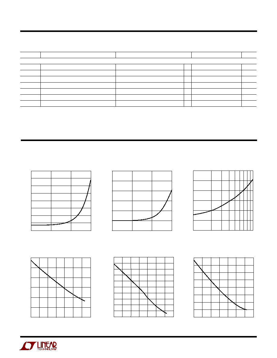
TYPICAL PERFOR A CE CHARACTERISTICS
U
W
V.11 Mode I
CC
vs Data Rate
DATA RATE (kBd)
10
I
CC
(mA)
120
130
140
2846 G04
110
100
90
100
1000
150
160
170
10000
T
A
= 25
∞
C
DATA RATE (kBd)
10
120
I
CC
(mA)
125
130
135
140
150
100
1000
2846 G05
10000
145
T
A
= 25
∞
C
DATA RATE (kBd)
10
30
I
CC
(mA)
35
40
45
50
60
20
40
60
80 100
2846 G06
55
T
A
= 25
∞
C
V.35 Mode I
CC
vs Data Rate
V.28 Mode I
CC
vs Data Rate
V.11 Mode I
CC
vs Temperature
V.35 Mode I
CC
vs Temperature
V.28 Mode I
CC
vs Temperature
TEMPERATURE (
∞
C)
≠40
I
CC
(mA)
100
105
110
20
60
2846 G07
95
90
≠20
0
40
80
100
85
80
TEMPERATURE (
∞
C)
≠40
123.0
I
CC
(mA)
123.5
124.5
125.0
125.5
128.0
126.5
0
40
60
2846 G08
124.0
127.0
127.5
126.0
≠20
20
80
100
TEMPERATURE (
∞
C)
≠40
I
CC
(mA)
37.0
20
3846 G09
35.5
34.5
≠ 20
0
40
34.0
33.5
37.5
36.5
36.0
35.0
60
80
100