 | –≠–ª–µ–∫—Ç—Ä–æ–Ω–Ω—ã–π –∫–æ–º–ø–æ–Ω–µ–Ω—Ç: 3442 | –°–∫–∞—á–∞—Ç—å:  PDF PDF  ZIP ZIP |

LTC3442
1
3442f
, LTC and LT are registered trademarks of Linear Technology Corporation. All other
trademarks are the property of their respective owners. Burst Mode is a registered
trademark of Linear Technology Corporation. Protected by U.S. Patents including 6404251,
6166527.
SW1
V
IN
SHDN/SS
R
LIM
R
T
SGND
SW2
V
OUT
FB
V
C
BURST
PGND
LTC3442
10µF
0.01µF
V
IN
2.5V TO
4.2V
Li-Ion
340k
2.2k
22µF
220pF
V
OUT
3.3V
1.2A
200k
0.01µF
15k
470pF
3442 TA01a
4.7µH
1M
71.5k
200k
TYPICAL APPLICATIO
U
APPLICATIO S
U
FEATURES
DESCRIPTIO
U
Micropower Synchronous
Buck-Boost DC/DC Converter with
Automatic Burst Mode Operation
The LTC
Æ
3442 is a highly efficient, fixed frequency, Buck-
Boost DC/DC converter, which operates from input volt-
ages above, below, and equal to the output voltage. The
topology incorporated in the IC provides a continuous
transfer function through all operating modes, making the
product ideal for a single Lithium-Ion or multicell alkaline
applications where the output voltage is within the battery
voltage range.
The device includes two 0.10 N-channel MOSFET
switches and two 0.10 P-channel switches. Operating
frequency and average input current limit can each be
programmed with an external resistor. Quiescent current
is only 35µA in Burst Mode operation, maximizing battery
life in portable applications. Automatic Burst Mode opera-
tion allows the user to program the load current for Burst
Mode operation, or to control it manually.
Other features include 1µA shutdown current, program-
mable soft-start, peak current limit and thermal shutdown.
The LTC3442 is available in a low profile, thermally en-
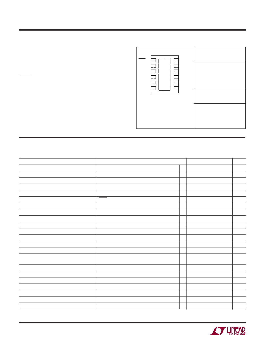
hanced 12-lead (4mm ◊ 3mm ◊ 0.75mm) DFN package.
PDA/`SMART' Phones
Handheld Computers
MP3 Players
Handheld Instruments
Digital Cameras
Wireless Handsets
USB Peripherals
Efficiency vs V
IN
V
IN
(V)
2.5
EFFICIENCY (%)
100
90
80
70
60
50
3.0
3.5
4.0
4.5
3442 ∑ TA01b
5.0
5.5
1A LOAD
300mA LOAD
V
OUT
= 3.3V
L = 4.7µH
F = 600kHz
Regulated Output with Input Voltages Above,
Below, or Equal to the Output
Single Inductor, No Schottky Diodes Required
Manual or Programmable Automatic Burst Mode
Æ
Operation
Programmable Average Input Current Limit
Up to 1.2A Continuous Output Current from a Single
Lithium-Ion Cell
High Efficiency: Up to 95%
Output Disconnect in Shutdown
2.4V to 5.5V Input Range
2.4V to 5.25V Output Range
35µA Quiescent Current in Burst Mode Operation
Programmable Frequency from 300kHz to 2MHz
<1µA Shutdown Current
Small, Thermally Enhanced 12-Lead (4mm ◊ 3mm)
DFN Package
LTC3442
2
3442f
V
IN
, V
OUT
Voltage ........................................... ≠ 0.3 to 6V
SW1, SW2 Voltage
DC ................................................................. ≠ 0.3 to 6V
Pulsed <100ns ............................................... ≠ 0.3 to 7V
SHDN/SS, BURST Voltage ............................. ≠ 0.3 to 6V
Operating Temperature (Note 2) ............. ≠ 40∞C to 85∞C
Maximum Junction Temperature (Note 4) ............ 125∞C
Storage Temperature Range ................. ≠ 65∞C to 125∞C
ORDER PART
NUMBER
DE PART
MARKING
3442
LTC3442EDE
ABSOLUTE AXI U
RATI GS
W
W
W
U
PACKAGE/ORDER I FOR ATIO
U
U
W
(Note 1)
ELECTRICAL CHARACTERISTICS
The
denotes the specifications which apply over the full operating
temperature range, otherwise specifications are at T
A
= 25∞C. V
IN
= V
OUT
= 3.6V, R
T
= 64.9k, unless otherwise noted.
PARAMETER
CONDITIONS
MIN
TYP
MAX
UNITS
Input Start-Up Voltage
2.3
2.4
V
Output Voltage Adjust Range
2.4
5.25
V
Feedback Voltage
1.19
1.22
1.25
V
Feedback Input Current
V
FB
= 1.22V
1
50
nA
Quiescent Current ≠ Burst Mode Operation
V
FB
= 1.22V, BURST = 0V (Note 3)
35
60
µA
Quiescent Current ≠ Shutdown
SHDN = 0V, V
OUT
= 0V, Not Including Switch Leakage
0.1
1
µA
Quiescent Current ≠ Active
BURST = V
IN
(Note 3)
600
1100
µA
NMOS Switch Leakage
Switches B and C
0.1
2
µA
PMOS Switch Leakage
Switches A and D
0.1
3
µA
NMOS Switch On Resistance
Switches B and C
0.10
PMOS Switch On Resistance
Switches A and D
0.10
Input Current Limit
2
3
A
Reverse Current Limit
0.5
A
Burst Mode Operation Current Limit
0.9
A
Max Duty Cycle
Boost (% Switch C On)
70
88
%
Buck (% Switch A In)
100
%
Min Duty Cycle
0
%
Frequency Accuracy
570
670
770
kHz
Error Amp A
VOL
90
dB
Error Amp Source Current
11
µA
Error Amp Sink Current
300
µA
Burst Threshold (Falling)
0.88
V
Burst Threshold (Rising)
1.12
V
T
JMAX
= 125∞C
JA
= 53∞C/W 1-Layer Board
JA
= 43∞C/W 4-Layer Board
JC
= 4.3∞C/W
EXPOSED PAD IS PGND (PIN 13)
MUST BE SOLDERED TO PCB
12
11
10
9
8
7
1
2
3
4
5
6
FB
V
C
R
LIM
V
IN
V
OUT
BURST
SHDN/SS
RT
SGND
SW1
PGND
SW2
TOP VIEW
13
DE12 PACKAGE
12-LEAD (4mm ◊ 3mm) PLASTIC DFN
LTC3442
3
3442f
V
IN
(V)
2.5
% CHANGE (NORMALIZED)
4.0
5.0
3442 G05
3.0
3.5
4.5
8
6
4
2
0
≠2
≠4
≠6
≠8
V
OUT
= 3.3V
1MHz
3442 G01
LOAD (mA)
0.1
EFFICIENCY (%)
1
10
100
1000
10000
90
60
100
80
70
50
40
30
20
Burst Mode
OPERATION
FIXED FREQUENCY
V
IN
= 5V
V
IN
= 3.3V
V
IN
= 2.5V
V
IN
= 5V
V
IN
= 3.3V
V
IN
= 2.5V
V
OUT
= 3.3V
600kHz
FREQUENCY (MHz)
0.50
% CHANGE (NORMALIZED)
0.75
1.00
1.25
1.50
3442 TA01b
1.75
15
10
5
0
≠5
≠10
2.00
V
IN
= 5V
V
OUT
SHORTED
V
OUT
DROPS 10%
PARAMETER
CONDITIONS
MIN
TYP
MAX
UNITS
Burst Current Ratio
Ratio of I
OUT
to I
BURST
20,000
Input Current Ratio
Ratio of I
IN
to I
RLIM
, I
IN
= 0.5A
70,000
R
LIM
Threshold
0.95
V
SHDN/SS Threshold
When IC is Enabled
0.4
0.7
1.4
V
When EA is at Max Boost Duty Cycle
2.2
2.4
V
SHDN/SS Input Current
V
SHDN
= 5.5V
0.01
1
µA
ELECTRICAL CHARACTERISTICS
The
denotes the specifications which apply over the full operating
temperature range, otherwise specifications are at T
A
= 25∞C. V
IN
= V
OUT
= 3.6V, R
T
= 64.9k, unless otherwise noted.
Note 1: Absolute Maximum Ratings are those values beyond which the life
of a device may be impaired.
Note 2: The LTC3442E is guaranteed to meet performance specifications
from 0∞C to 70∞C. Specifications over ≠40∞C to 85∞C operating
temperature range are assured by design, characterization and correlation
with statistical process controls.
Note 3: Current Measurements are performed when the outputs are not
switching.
Note 4: This IC includes overtemperature protection that is intended to
protect the device during momentary overload conditions. Junction
temperature will exceed 125∞C when overtemperature protection is active.
Continuous operation above the specified maximum operating junction
temperature may result in device degradation or failure.
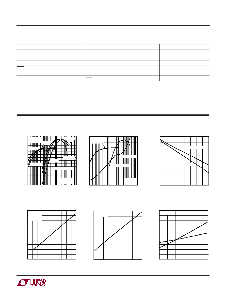
TYPICAL PERFOR A CE CHARACTERISTICS
U
W
Efficiency vs Load
Efficiency and Power Loss vs Load
Efficiency vs Frequency
Input Current Mirror Linearity
Average Input Current Limit
vs V
IN
(Normalized)
LOAD CURRENT (mA)
0.1
EFFICIENCY (%)
1
10
100
1000
10000
3442 G02
90
60
40
30
20
100
80
70
50
10
1
0.1
1000
100
POWER LOSS (mW)
Burst Mode
OPERATION
FIXED FREQUENCY
POWER LOSS
V
IN
= 3.6V
V
OUT
= 3.3V
FREQUENCY (kHz)
400
EFFICIENCY (%)
2000
3442 G03
800
1200
1600
600
1000
1400
1800
96
94
92
90
88
86
84
82
80
WITHOUT SCHOTTKY DIODES
WITH SCHOTTKY DIODES
V
IN
= 3.6V
V
OUT
= 3.3V
INPUT CURRENT (A)
0
1.00
0.90
0.80
0.60
0.70
0.50
0.40
0.30
0.20
0.10
0.00
.40
3442 G04
.10
.05
.15
.25
.35
.45
.20
.30
.50
R
LIM
VOLTAGE (V)
V
IN
= 3.6V
V
OUT
= 3.3V
R
LIM
= 133k
(T
A
= 25∞C unless otherwise specified).
Average Input Current Limit
vs Frequency (Normalized)

LTC3442
4
3442f
TYPICAL PERFOR A CE CHARACTERISTICS
U
W
(T
A
= 25∞C unless otherwise specified).
Quiescent Current vs V
IN
(Fixed Frequency Mode)
Burst Mode Quiescent Current
vs V
IN
Peak Current Clamp vs V
IN
V
IN
(V)
2.5
V
IN
QUIESCENT CURRENT (mA)
4.0
5.0
3442 G07
3.0
3.5
4.5
4.0
3.5
3.0
2.5
2.0
1.5
1.0
0.5
0.0
5.5
2.0 MHz
1.5 MHz
1.0 MHz
0.5 MHz
NO SWITCHING
V
IN
(V)
2.5
V
IN
QUIESCENT CURRENT (
µ
A)
3.0
3.5
4.0
4.5
3442 G08
5.0
50
45
40
35
30
25
20
15
10
5
0
5.5
V
IN
(V)
2.5
2.0
2.5
3.0
4.0
5.0
3442 G09
1.5
1.0
3.0
3.5
4.5
5.5
0.5
0.0
INPUT CURRENT (A)
3.5
Automatic Burst Mode Threshold
vs R
BURST
Minimum Start Voltage
vs Temperature
Average Input Current Limit
vs Temperature (Normalized)
Frequency Change vs Temperature
(Normalized)
Feedback Voltage vs Temperature
(Normalized)
Switch Pins Before Entering
Boost Mode
R
BURST
(k)
150
60
LOAD CURRENT (mA)
70
90
100
110
160
130
175
225
3442 G10
80
140
150
120
200
250
ENTER Burst Mode
OPERATION
LEAVE Burst Mode
OPERATION
TEMPERATURE (∞C)
≠55
MINIMUM START VOLTAGE (V)
≠25
5
35
65
3442 G11
95
2.30
2.29
2.28
2.27
2.26
2.25
2.24
2.23
2.22
2.21
2.20
125
TEMPERATURE (∞C)
≠55
CHANGE FROM 25
∞
C
5%
4%
3%
2%
1%
0%
≠1%
≠2%
≠3%
≠4%
≠5%
≠15
25
45
125
3442 G12
≠35
5
65
85 105
V
IN
= V
OUT
= 3.3V
TEMPERATURE (∞C)
≠55
CHANGE FROM 25
∞
C
0.0%
0.5%
1.0%
105
3442 G13
≠0.5%
≠1.0%
≠2.0%
≠15
25
65
≠35
125
5
45
85
≠1.5%
2.0%
1.5%
TEMPERATURE (∞C)
≠55
CHANGE FROM 25
∞
C
1.0%
0.8%
0.6%
0.4%
0.2%
0.0%
≠2.0%
≠0.4%
≠0.6%
≠0.8%
≠1.0%
≠15
25
45
125
3442 G14
≠35
5
65
85 105
V
IN
= V
OUT
= 3.3V
50ns/DIV
3442 G15
SW1
2V/DIV
SW2
2V/DIV
V
IN
= 2.9V
V
OUT
= 3.3V AT 500mA

LTC3442
5
3442f
200µs/DIV
3442 G22
C
OUT
= 100µF
LOW ESR TANTALUM
INDUCTOR
CURRENT
0.5A/DIV
V
OUT
50mV/DIV
1ms/DIV
3442 G23
R
LIM
= 133k
C
LIM
= .001µF
INDUCTOR
CURRENT
0.5A/DIV
R
LIM
PIN
0.5V/DIV
V
OUT
2V/DIV
20µs/DIV
3442 G21
C
OUT
= 100µF
LOW ESR TANTALUM
INDUCTOR
CURRENT
0.5A/DIV
V
OUT
50mV/DIV
50ns/DIV
3442 G17
SW1
2V/DIV
SW2
2V/DIV
V
IN
= 4.2V
V
OUT
= 3.3V AT 500mA
50ns/DIV
3442 G16
SW1
2V/DIV
SW2
2V/DIV
V
IN
= 3.3V
V
OUT
= 3.3V AT 500mA
TYPICAL PERFOR A CE CHARACTERISTICS
U
W
Switch Pins in Buck-Boost Mode
Switch Pins Entering
Buck-Boost Mode
Output Ripple at 1A Load
Load Transient Response in Fixed
Frequency Mode, No Load to 1A
Load Transient Response in Auto
Burst Mode Operation, No Load to 1A
Burst Mode Operation
Pulsed Overload Using Average
Input Current Limit
Transition from Burst Mode
Operation to Fixed Frequency Mode
1µs/DIV
3442 G18
V
OUT
20mV/DIV
AC COUPLED
V
IN
= 4.2V
V
IN
= 3.3V
V
IN
= 2.7V
100µs/DIV
3442 G19
V
IN
= 3.6V
V
OUT
= 3.3V
C
OUT
= 47µF, X5R CERAMIC
LOAD
0.5A/DIV
V
OUT
100mV/DIV
100µs/DIV
3442 G20
V
IN
= 3.6V
V
OUT
= 3.3V
C
OUT
= 47µF, X5R CERAMIC + 100µF
LOW ESR TANTALUM
LOAD
0.5A/DIV
V
OUT
100mV/DIV
(T
A
= 25∞C unless otherwise specified).