 | –≠–ª–µ–∫—Ç—Ä–æ–Ω–Ω—ã–π –∫–æ–º–ø–æ–Ω–µ–Ω—Ç: LT1002 | –°–∫–∞—á–∞—Ç—å:  PDF PDF  ZIP ZIP |
1
LT1002
Dual, Matched Precision
Operational Amplifier
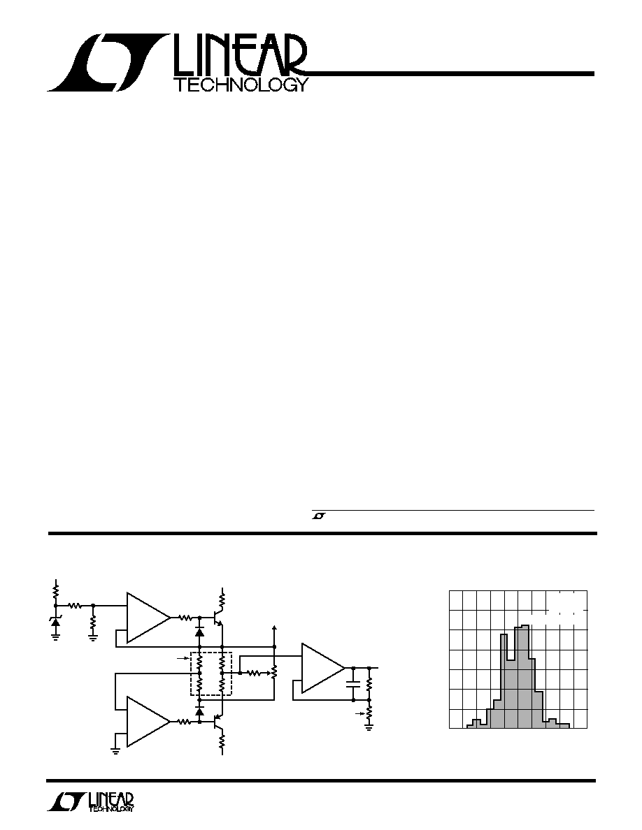
Strain Gauge Signal Conditioner with Bridge Excitation
≠
+
LT1001
3
10
4
11
13
6
2.0K*
8.2k
LM329
+15V
2
3
6
1002 TA01
2k
4.99k*
2k
≠15V
*RN60C FILM RESISTORS
+15V
IN4148
350
BRIDGE
2N2219
REFERENCE OUT
TO MONITORING
A/D CONVERTER
IN4148
100
5W
100
5W
10k
ZERO
1
µ
F
340k*
0 TO 10V
OUT
*
301k
1.1k*
2N2907
≠
+
1
/
2
LT1002
≠
+
1
/
2
LT1002
GAIN
TRIM
INPUT OFFSET VOLTAGE MATCH (
µ
V)
≠100
NUMBER OF UNITS
70
60
50
40
30
20
10
0
≠80
0
40
1002 TA02
≠20
80 100
≠60 ≠40
20
60
V
S
=
±
15V
T
A
= 25
∞
C
287 UNITS TESTED
Distribution of Offset Voltage Match
FEATURES
APPLICATIO
N
S
U
s
Thermocouple Amplifiers
s
Strain Gauge Amplifiers
s
Low level signal processing
s
Medical instrumentation
s
Precision dual limit threshold detection
s
Instrumentation amplifiers
s
Guaranteed low offset voltage
LT1002A
60
µ
V max
LT1002
100
µ
V max
s
Guaranteed offset voltage match
LT1002A
40
µ
V max
LT1002
80
µ
V max
s
Guaranteed low drift
LT1002A
0.9
µ
V/
∞
C max
LT1002
1.3
µ
V/
∞
C max
s
Guaranteed CMRR
LT1002A
110dB min
LT1002
110dB min
s
Guaranteed channel separation
LT1002A
132dB min
LT1002
130dB min
s
Guaranteed maching characteristics
s
Low noise 0.35
µ
V p-p
DESCRIPTIO
N
U
The LT
Æ
1002 dual, matched precision operational amplifiers
combine excellent individual amplifier performance with tight
matching and temperature tracking between amplifiers.
In the design, processing, and testing of the device, particular
attention has been paid to the optimization of the entire
distribution of several key parameters and their matching.
Consequently, the specifications of even the low cost commer-
cial grade (the LT1002C) have been spectacularly improved
compared to presently available devices.
Essentially, the input offset voltage of all units is less than
80
µ
V, and matching between amplifiers is consistently beter
than 60
µ
V (see distribution plot below). Input bias and offset
currents, channel separation, common mode and power suply
rejections of the LT1002C are all specified at levels which were
previsouly attainable only on very expensive, selected grades
of other dual devices. Power dissipation is nearly halved
compared to the most popular precision duals, without ad-
versely affecting noise or speed performance. A by-product of
lower dissipation is decreased warm-up drift. For even better
performance in a single precision op amp, refer to the LT1001
data sheet. A bridge signal conditioning application is shown
below. This circuit illustrates the requirement for both excel-
lent matching and individual amplifier specifications.
, LTC and LT are registered trademarks of Linear Technology Corporation.

2
LT1002
LT1002AM/LT1002AC
LT1002M/LT1002C
SYMBOL
PARAMETER
CONDITIONS
MIN
TYP
MAX
MIN
TYP
MAX
UNITS
V
OS
Input Offset Voltage
Note 1
20
60
25
100
µ
V
V
OS
Long Term Input Offset Voltage
Time
Stability
Notes 2 and 3
0.3
1.5
0.4
2.0
µ
V/month
I
OS
Input Offset Current
0.3
2.8
0.4
4.2
nA
I
B
Input Bias Current
±
0.6
±
3.0
±
0.7
±
4.5
nA
e
n
Input Noise Voltage
0.1Hz to 10Hz (Note 2)
0.35
0.7
0.38
0.75
µ
V
p-p
e
n
Input Noise Voltage Density
f
O
= 10Hz (Note 5)
10.3
20.0
10.5
20.0
f
O
= 1000Hz (Note 2)
9.6
11.5
9.8
12.0
nV
Hz
A
VOL
Large Signal Voltage Gain
R
L
2k
, V
O
=
±
12V
400
800
350
800
V/mV
R
L
1k
, V
O
=
±
10V
250
500
220
500
CMRR
Common Mode Rejection Ratio
V
CM
=
±
13V
110
126
110
126
dB
PSRR
Power Supply Rejection Ratio
V
S
=
±
3V to
±
18V
108
123
105
123
dB
R
in
Input Resistance Differential Mode
Note 4
20
100
13
80
M
Input Voltage Range
±
13
±
14
±
13
±
14
V
V
OUT
Maximum Output Voltage Swing
R
L
2k
±
13
±
14
±
13
±
14
V
R
L
1k
±
12
±
13.5
±
12
±
13.5
SR
Slew Rate
R
L
2k
(Note 4)
0.1
0.25
0.1
0.25
V/
µ
s
GBW
Gain Bandwidth Product
Note 4
0.4
0.8
0.4
0.8
MHz
P
d
Power Dissipation
No load
46
75
48
85
mW
per amplifier
No load, V
S
=
±
3V
4
7
4
8
ABSOLUTE
M
AXI
M
U
M
RATINGS
W
W
W
U
Supply Voltage (Note 6).........................................
±
22V
Differential Input Voltage ......................................
±
30V
Input Voltage Equal to Supply Voltage
Output Short Circuit Duration ......................... Indefinite
Operating Temperature Range
LT1002AM/LT1002M ....................... ≠ 55
∞
C to 125
∞
C
LT1002AC/LT1002C ............................... 0
∞
C to 70
∞
C
Storage Temperature Range
All Grades ......................................... ≠ 65
∞
C to 150
∞
C
Lead Temperature (Soldering, 10 sec.)................. 300
∞
C
PACKAGE/ORDER I
N
FOR
M
ATIO
N
W
U
U
1
2
3
4
5
6
7
TOP VIEW
J PACKAGE
14 PIN HERMETIC
N PACKAGE
14 PIN PLASTIC
14
13
12
11
10
9
8
NULL (A)
NULL (A)
≠IN (A)
+IN (A)
V≠ (B)
OUT (B)
V+ (B)
V+ (A)
OUT (A)
V≠ (A)
+IN (B)
≠IN (B)
NULL (B)
NULL (B)
≠
≠
+
+
A
B
LT1002AMJ
LT1002MJ
LT1002ACJ
LT1002CJ
LT1002ACN
LT1002CN
OFFSET
VOLTAGE
MAX
at 25
∞
C
ORDER
PART NO.
60
µ
V
100
µ
V
60
µ
V
100
µ
V
60
µ
V
100
µ
V
NOTE: Device may be operated even if insertion
is reversed; this is due to inherent symmetry of
pin locations of amplifiers A and B. (Note 6)
ELECTRICAL CHARACTERISTICS, I DIVIDUAL A PLIFIERS
U
W
V
S
=
±
15V, T
A
= 25
∞
C, unless otherwise noted
3
LT1002
ELECTRICAL CHARACTERISTICS, I DIVIDUAL A PLIFIERS
U
W
V
S
=
±
15V, ≠ 55
∞
C
T
A
125
∞
C, unless otherwise noted
LT1002AM
LT1002M
SYMBOL
PARAMETER
CONDITIONS
MIN
TYP
MAX
MIN
TYP
MAX
UNITS
V
OS
Input Offset Voltage
Note 1
q
30
150
45
230
µ
V
V
OS
Average Input Offset Voltage Drift
q
0.2
0.9
0.3
1.3
µ
V/
∞
C
Temp
I
OS
Input Offset Current
q
0.8
5.6
1.2
8.5
nA
I
B
Input Bias Current
q
±
1.0
±
6.0
±
1.5
±
9.0
nA
A
VOL
Large Signal Voltage Gain
R
L
2k
, V
O
=
±
10V
q
300
700
200
700
V/mV
CMRR
Common Mode Rejection Ratio
V
CM
=
±
13V
q
106
122
104
120
dB
PSRR
Power Supply Rejection Ratio
V
S
=
±
3V to
±
18V
q
102
117
96
117
dB
Input Voltage Range
q
±
13
±
14
±
13
±
14
V
V
OUT
Output Voltage Swing
R
L
2k
q
±
12.5
±
13.5
±
12.0
±
13.5
V
P
d
Power Dissipation
No load
q
55
90
60
100
mW
per amplifier
LT1002AC
LT1002C
SYMBOL
PARAMETER
CONDITIONS
MIN
TYP
MAX
MIN
TYP
MAX
UNITS
V
OS
Input Offset Voltage
Note 1
q
20
100
30
160
µ
V
V
OS
Average Input Offset Voltage Drift
q
0.2
0.9
0.3
1.3
µ
V/
∞
C
Temp
I
OS
Input Offset Current
q
0.5
4.2
0.6
5.7
nA
I
B
Input Bias Current
q
±
0.7
±
4.5
±
1.0
±
6.0
nA
A
VOL
Large Signal Voltage Gain
R
L
2k
, V
O
=
±
10V
q
350
750
250
750
V/mV
CMRR
Common Mode Rejection Ratio
V
CM
=
±
13V
q
108
124
106
123
dB
PSRR
Power Supply Rejection Ratio
V
S
=
±
3V to
±
18V
q
105
120
100
120
dB
Input Voltage Range
q
±
13
±
14
±
13
±
14
V
V
OUT
Output Voltage Swing
R
L
2k
q
±
12.5
±
13.8
±
12.5
±
13.8
V
P
d
Power Dissipation
No Load
q
50
85
55
90
mW
per amplifier
V
S
=
±
15V, 0
∞
C
T
A
70
∞
C, unless otherwise noted
The
q
denotes the specifications which apply over the full operating
temperature range.
For MIL-STD components, please refer to LTC 883C data sheet for test
listing and parameters.
Note 1: Offset voltage measured with high speed test equipment,
approximately 1second after power is applied.
Note 2: This parameter is tested on a sample basis only.
Note 3: Long Term Input Offset Voltage Stability refers to the averaged
trend line of V
OS
versus Time over extended periods after the first 30 days
of operation. Excluding the initial hour of operation, changes in V
OS
during
the first 30 operating days are typically 2.5
µ
V.
Note 4: Parameter is guaranteed by design.
Note 5: 10Hz noise voltage density is sample tested on every lot.
Devices 100% tested at 10Hz are available on request.
Note 6: The V + supply terminals are completely independent and may be
powered by separate supplies if desired (this approach, however, would
sacrifice the advantages of the power supply rejection ratio matching). The
V ≠ supply terminals are both connected to the common substrate and
must be tied to the same voltage. Both V ≠ pins should be used.
4
LT1002
at V
S
=
±
15V, T
A
= 25
∞
C, unless otherwise noted
LT1002AM/AC
LT1002M/C
SYMBOL
PARAMETER
CONDITIONS
MIN
TYP
MAX
MIN
TYP
MAX
UNITS
Input Offset Voltage Match
≠
15
40
≠
25
80
µ
V
I
B
+
Average Non-Inverting Bias
Current
≠
±
0.6
±
3.5
≠
±
0.7
±
4.8
nA
I
OS
+
Non-Inverting Offset Current
≠
0.6
3.5
≠
0.7
6.0
nA
I
OS
≠
Inverting Offset Current
≠
0.6
3.5
≠
0.7
6.0
nA
CMRR
Common Mode Rejection Ratio
Match
V
CM
=
±
13V
110
132
≠
108
132
≠
dB
PSRR
Power Supply Rejection Ratio
Match
V
S
=
±
3V to
±
18V
108
130
≠
102
128
≠
dB
Channel Seperation
f
10Hz (Note 4)
132
148
≠
130
146
≠
dB
ATCHI G CHARACTERISTICS
U
W
at V
S
=
±
15V, ≠ 55
∞
C
T
A
125
∞
C, unless otherwise noted
LT1002AM
LT1002M
SYMBOL
PARAMETER
CONDITIONS
MIN
TYP
MAX
MIN
TYP
MAX
UNITS
Input Offset Voltage Match
q
≠
50
140
≠
60
230
µ
V
Input Offset Voltage Tracking
q
≠
0.3
1.0
≠
0.4
1.5
µ
V/
∞
C
I
B
+
Average Non-Inverting Bias
Current
q
≠
±
1.5
±
6.0
≠
±
1.8
±
10.0
nA
I
OS
+
Non-Inverting Offset Current
q
≠
1.5
6.5
≠
1.8
12.0
nA
I
OS
≠
Inverting Offset Current
q
≠
1.5
6.5
≠
1.8
12.0
nA
CMRR
Common Mode Rejection Ratio
Match
V
CM
=
±
13V
q
106
126
102
124
≠
dB
PSRR
Power Supply Rejection Ratio
Match
V
S
=
±
3V to
±
18V
q
102
122
94
120
≠
dB
ATCHI G CHARACTERISTICS
U
W
at V
S
=
±
15V, 0
∞
C
T
A
70
∞
C, unless otherwise noted
LT1002AC
LT1002C
SYMBOL
PARAMETER
CONDITIONS
MIN
TYP
MAX
MIN
TYP
MAX
UNITS
Input Offset Voltage Match
q
≠
30
85
≠
45
150
µ
V
Input Offset Voltage Tracking
q
≠
0.3
1.0
≠
0.4
1.5
µ
V/
∞
C
I
B
+
Average Non-Inverting Bias
Current
q
≠
±
1.0
±
4.5
≠
±
1.2
±
7.0
nA
I
OS
+
Non-Inverting Offset Current
q
≠
1.0
5.0
≠
1.2
8.5
nA
I
OS
≠
Inverting Offset Current
q
≠
1.0
5.0
≠
1.2
8.5
nA
CMRR
Common Mode Rejection Ratio
Match
V
CM
=
±
13V
q
108
130
≠
105
128
≠
dB
PSRR
Power Supply Rejection Ratio
Match
V
S
=
±
3V to
±
18V
q
105
126
≠
98
124
≠
dB
ATCHI G CHARACTERISTICS
U
W

5
LT1002
TYPICAL PERFOR
M
A
N
CE CHARACTERISTICS
U
W
Distribution of Offset Voltage
Match Drift with Temperature
INPUT OFFSET VOLTAGE DRIFT
WITH TEMPERATURE (
µ
V/
∞
C)
NUMBER OF UNITS
70
60
50
40
30
20
10
0
1002 G02
≠1.2
≠0.8
≠0.4
0
+0.4
+0.8
+1.2
260 UNITS TESTED
V
S
=
±
15V
Offset Voltage Drift with Temperature
of Six Representative Units
Offset Voltage Tracking with Temperature
of Six Representative Units
Long Term Stability of Four
Representative Units
TIME (MONTHS)
0
OFFSET VOLTAGE CHANGE (
µ
V)
4
1001 G07
1
2
3
5
10
5
0
≠5
≠10
FREQUENCY (Hz)
1
1
3
10
30
100
0.1
1
3
10
10
100
1000
1002 G09
VOLTAGE NOISE nV/
Hz
T
A
= 25
∞
C
V
S
=
±
3 TO
±
18V
VOLTAGE
CURRENT
1/f CORNER
70Hz
1/f CORNER
4Hz
0.3
CURRENT NOISE pA/
Hz
TIME (SECONDS)
0
NOISE VOLTAGE 100nV/DIV
8
1001 G08
2
4
6
10
Distribution of Offset Voltage Drift
with Temperature
(Individual Amplifiers)
Distribution of Offset Voltage of
Individual Amplifiers
OFFSET VOLTAGE MATCH DRIFT
WITH TEMPERATURE (
µ
V/
∞
C)
NUMBER OF UNITS
35
30
25
20
15
10
5
1002 G03
≠1.2
≠0.8
≠0.4
0
+0.4
+0.8
+1.2
130 UNITS TESTED
V
S
=
±
15V
Warm-Up Drift
TIME AFTER POWER ON ≠
BOTH AMPLIFIERS (MINUTES)
0
CHANGE IN OFFSET VOLTAGE (MICROVOLTS)
5
4
3
2
1
0
4
1002 G06
1
2
3
5
V
S
=
±
15V
T
A
= 25
∞
C
N14 PLASTIC PACKGE
J14 HERMETIC DIP PACKGE
TEMPERATURE (
∞
C)
≠50
OFFSET VOLTAGE MATCH (
µ
V)
100
80
60
40
20
0
≠20
≠40
≠60
≠80
≠100
0
50
75
1002 G04
≠25
25
100
125
LT1002AM
LT1002AM
LT1002AM
LT1002M
LT1002M
V
S
=
±
15V
LT1002M
TEMPERATURE (
∞
C)
≠50
INDIVIDUAL AMPLIFIER OFFSET VOLTAGE (
µ
V)
100
80
60
40
20
0
≠20
≠40
≠60
≠80
≠100
0
50
75
1002 G04
≠25
25
100
125
LT1002AM
LT1002AM
LT1002AM
LT1002M
LT1002M
LT1002M
0.1Hz to 10Hz Noise
Noise Spectrum
INPUT OFFSET VOLTAGE (
µ
V)
≠100 ≠80
NUMBER OF UNITS
100
80
60
40
20
0
60
1002 G01
≠60 ≠40 ≠20 0
20 40
80 100
574 UNITS TESTED
V
S
=
±
15V
T
A
= 25
∞
C