 | –≠–ª–µ–∫—Ç—Ä–æ–Ω–Ω—ã–π –∫–æ–º–ø–æ–Ω–µ–Ω—Ç: LT1071 | –°–∫–∞—á–∞—Ç—å:  PDF PDF  ZIP ZIP |

1
LT1070/LT1071
5A and 2.5A High Efficiency
Switching Regulators
s
Wide Input Voltage Range: 3V to 60V
s
Low Quiescent Current: 6mA
s
Internal 5A Switch (2.5A for LT1071)
s
Very Few External Parts Required
s
Self Protected Against Overloads
s
Operates in Nearly All Switching Topologies
s
Shutdown Mode Draws Only 50
µ
A Supply Current
s
Flyback Regulated Mode Has Fully Floating Outputs
s
Comes in Standard 5-Pin Packages
s
Can be Externally Synchronized (Consult Factory)
FEATURES
The LT
Æ
1070/LT1071 are monolithic high power switch-
ing regulators. They can be operated in all standard switch-
ing configurations including buck, boost, flyback, for-
ward, inverting and "Cuk". A high current, high efficiency
switch is included on the die along with all oscillator,
control and protection circuitry. Integration of all func-
tions allows the LT1070/LT1071 to be built in a standard
5-pin TO-3 or T0-220 power package. This makes it ex-
tremely easy to use and provides "bust proof" operation
similar to that obtained with 3-pin linear regulators.
The LT1070/LT1071 operate with supply voltages from 3V
to 60V, and draw only 6mA quiescent current. They can
deliver load power up to 100W with no external power
devices. By utilizing current mode switching techniques,
they provide excellent AC and DC load and line regulation.
The LT1070/LT1071 have many unique features not found
even on the vastly more difficult to use low power control
chips presently available. They use adaptive antisat switch
drive to allow very wide ranging load currents with no loss
in efficiency. An externally activated shutdown mode
reduces total supply current to 50
µ
A typical for standby
operation. Totally isolated and regulated outputs can be
generated by using the optional "flyback regulation mode"
built into the LT1070/LT1071, without the need for
optocouplers or extra transformer windings.
DESCRIPTIO
N
U
USER NOTE:
This data sheet is only intended to provide specifications, graphs and a general functional
description of the LT1070/LT1071. Application circuits are included to show the capability of the
LT1070/LT1071. A complete design manual (AN19) should be obtained to assist in developing new
designs. This manual contains a comprehensive discussion of both the LT1070 and the external
components used with it, as well as complete formulas for calculating the values of these
components. The manual can also be used for the LT1071 by factoring in the lower switch current
rating. A second Application Note, AN25, which details off-line applications is available.
TYPICAL APPLICATIO
N
U
+
R1
10.7k
1%
R2
1.24k
1%
1070/71 TA01
12V
1A
R3
1k
C1
1
µ
F
C2
1000
µ
F
+
C3*
100
µ
F
L1**
150
µ
H
D1
5V
V
SW
V
C
V
IN
LT1070
GND
FB
C3
100
µ
F
L2
10
µ
H
OUTPUT
FILTER
*
**
REQUIRED IF INPUT LEADS
2"
PULSE ENGINEERING 92113
INPUT VOLTAGE (V)
0
POWER (W)**
60
80
100
40
1070/71 TA02
40
20
0
10
20
30
50
BOOST
BUCK/BOOST
V
O
= 30V
FLYBACK
ISOLATED
BUCK/BOOST
V
O
= 5V
ROUGH GUIDE ONLY. BUCK MODE P
OUT
= 5A ∑ V
OUT
.
SPECIAL TOPOLOGIES DELIVER MORE POWER
DIVIDE VERTICAL POWER SCALE BY 2 FOR LT1071
*
**
Maximum Output Power*
Boost Converter (5V to 12V)
APPLICATIO
N
S
U
s
Logic Supply 5V at 10A
s
5V Logic to
±
15V Op Amp Supply
s
Off-Line Converter Up to 200W
s
Battery Upconverter
s
Power Inverter (+ to ≠) or (≠ to +)
s
Fully Floating Multiple Outputs
s
For Lower Current Applications, See the LT1072
, LTC and LT are registered trademarks of Linear Technology Corporation.
2
LT1070/LT1071
SYMBOL
PARAMETER
CONDITIONS
MIN
TYP
MAX
UNITS
V
REF
Reference Voltage
Measured at Feedback Pin, V
C
= 0.8V
1.224
1.244
1.264
V
q
1.214
1.244
1.274
V
I
B
Feedback Input Current
V
FB
= V
REF
350
750
nA
q
1100
nA
g
m
Error Amplifier Transconductance
I
C
=
±
25
µ
A
3000
4400
6000
µ
mho
q
2400
7000
µ
mho
Error Amplifier Source or Sink Current
V
C
= 1.5V
150
200
350
µ
A
q
120
400
µ
A
Error Amplifier Clamp Voltage
Hi Clamp, V
FB
= 1V
1.80
2.30
V
Lo Clamp, V
FB
= 1.5V
0.25
0.38
0.52
V
Reference Voltage Line Regulation
3V
V
IN
V
MAX
, V
C
= 0.8V
q
0.03
%/V
A
V
Error Amplifier Voltage Gain
0.9V
V
C
1.4V
500
800
V/V
Minimum Input Voltage
q
2.6
3.0
V
I
Q
Supply Current
3V
V
IN
V
MAX
, V
C
= 0.6V
6
9
mA
Control Pin Threshold
Duty Cycle = 0
0.8
0.9
1.08
V
q
0.6
1.25
V
Normal/Flyback Threshold on Feedback Pin
0.4
0.45
0.54
V
ABSOLUTE
M
AXI
M
U
M
RATINGS
W
W
W
U
Supply Voltage
LT1070/LT1071 (Note 2) .................................... 40V
LT1070HV/LT1071HV (Note 2)........................... 60V
Switch Output Voltage
LT1070/LT1071 .................................................. 65V
LT1070HV/LT1071HV......................................... 75V
Feedback Pin Voltage (Transient, 1ms) ................
±
15V
Operating Junction Temperature Range
Commercial (Operating) ....................... 0
∞
C to 100
∞
C
Commercial (Short Circuit)................... 0
∞
C to 125
∞
C
Industrial ......................................... ≠ 40
∞
C to 125
∞
C
Military ............................................ ≠ 55
∞
C to 150
∞
C
Storage Temperature Range ................ ≠ 65
∞
C to 150
∞
C
Lead Temperature (Soldering, 10 sec)................. 300
∞
C
PACKAGE/ORDER I
N
FOR
M
ATIO
N
W
U
U
ORDER PART
NUMBER
LT1070CK
LT1070HVCK
LT1070HVMK
LT1070IK
LT1070MK
LT1071CK
LT1071HVCK
LT1071HVMK
LT1071MK
ORDER PART
NUMBER
LT1070CT
LT1070HVCT
LT1070HVIT
LT1070IT
LT1071CT
LT1071HVCT
LT1071HVIT
LT1071IT
T
JMAX
= 100
∞
C,
JA
= 35
∞
C/ W, Q
JC
= 2
∞
C (LT1070C, I)
T
JMAX
= 150
∞
C,
JA
= 35
∞
C/ W, Q
JC
= 2
∞
C (LT1070M)
T
JMAX
= 100
∞
C,
JA
= 35
∞
C/ W, Q
JC
= 4
∞
C (LT1071C, I)
T
JMAX
= 150
∞
C,
JA
= 35
∞
C/ W, Q
JC
= 4
∞
C (LT1071M)
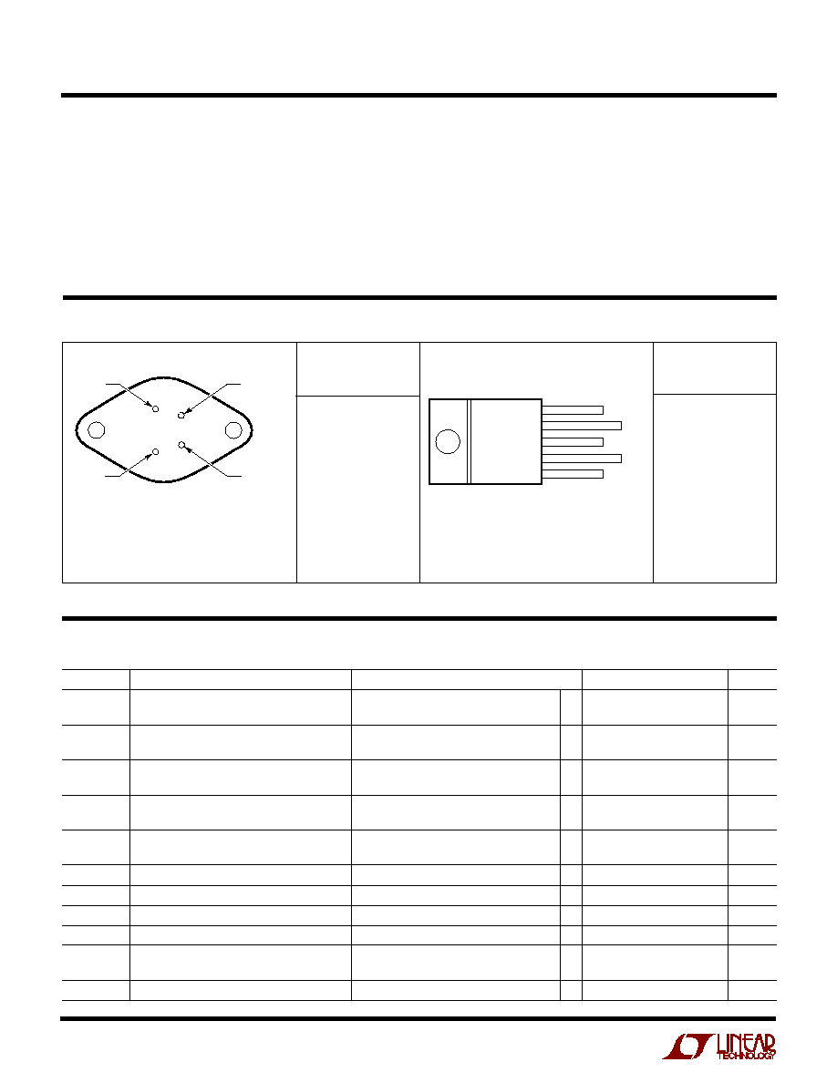
2
4
1
3
V
SW
V
C
FB
CASE
IS GND
V
IN
K PACKAGE
4-LEAD TO-3 METAL CAN
BOTTOM VIEW
T
JMAX
= 100
∞
C,
JA
= 75
∞
C/ W, Q
JC
= 2
∞
C (LT1070C, I)
T
JMAX
= 100
∞
C,
JA
= 75
∞
C/ W, Q
JC
= 4
∞
C (LT1071C)
T PACKAGE
5-LEAD PLASTIC TO-220
V
IN
V
SW
GND
FB
V
C
FRONT VIEW
5
4
3
2
1
ELECTRICAL CHARACTERISTICS
V
IN
= 15V, V
C
= 0.5V, V
FB
= V
REF
, output pin open unless otherwise specified.
(Note 1)
3
LT1070/LT1071
ELECTRICAL CHARACTERISTICS
SYMBOL
PARAMETER
CONDITIONS
MIN
TYP
MAX
UNITS
V
FB
Flyback Reference Voltage
I
FB
= 50
µ
A
15
16.3
17.6
V
q
14
18.0
V
Change in Flyback Reference Voltage
0.05
I
FB
1mA
4.5
6.8
8.5
V
Flyback Reference Voltage Line Regulation
I
FB
= 50
µ
A, 3V
V
IN
V
MAX
(Note 3)
0.01
0.03
%/V
Flyback Amplifier Transconductance (g
m
)
I
C
=
±
10
µ
A
150
300
650
µ
mho
Flyback Amplifier Source and Sink Current
V
C
= 0.6V, I
FB
= 50
µ
A (Source)
q
15
32
70
µ
A
V
C
= 0.6V, I
FB
= 50
µ
A (Sink)
q
25
40
70
µ
A
B
V
Output Switch Breakdown Voltage
3V
V
IN
V
MAX
,
I
SW
= 1.5mA
(LT1070/LT1071)
q
65
90
V
(LT1070HV/LT1071HV)
q
75
90
V
V
SAT
Output Switch "On" Resistance (Note 4)
LT1070
q
0.15
0.24
LT1071
q
0.30
0.50
Control Voltage to Switch Current
LT1070
8
A/V
Transconductance
LT1071
4
A/V
I
LIM
Switch Current Limit (LT1070)
Duty Cycle
50%, T
J
25
∞
C
q
5
10
A
Duty Cycle
50%, T
J
< 25
∞
C
q
5
11
A
Duty Cycle = 80% (Note 5)
q
4
10
A
Switch Current Limit (LT1071)
Duty Cycle
50%, T
J
25
∞
C
q
2.5
5.0
A
Duty Cycle
50%, T
J
< 25
∞
C
q
2.5
5.5
A
Duty Cycle = 80% (Note 5)
q
2.0
5.0
A
I
IN
Supply Current Increase During
25
35
mA/A
I
SW
Switch "On" Time
f
Switching Frequency
35
40
45
kHz
q
33
47
kHz
DC (Max)
Maximum Switch Duty Cycle
90
92
97
%
Flyback Sense Delay Time
1.5
µ
s
Shutdown Mode Supply Current
3V
V
IN
V
MAX
, V
C
= 0.05V
100
250
µ
A
Shutdown Mode Threshold Voltage
3V
V
IN
V
MAX
100
150
250
mV
q
50
300
mV
V
IN
= 15V, V
C
= 0.5V, V
FB
= V
REF
, output pin open unless otherwise specified.
The
q
denotes the specifications which apply over the full operating
temperature range.
Note 1: Absolute Maximum Ratings are those values beyond which the life of
a device may be impaired.
Note 2: Minimum switch "on" time for the LT1070/LT1071 in current limit is
1
µ
s. This limits the maximum input voltage during short-circuit conditions,
in the buck and inverting modes only, to
35V. Normal (unshorted) conditions
are not affected. Mask changes are being implemented which will reduce
minimum "on" time to
1
µ
s, increasing maximum short-circuit input voltage
above 40V. If the present LT1070/LT1071 (contact factory for package date
code) is being operated in the buck or inverting mode at high input voltages
and short-circuit conditions are expected, a resistor must be placed in series
with the inductor, as follows:
The value of the resistor is given by:
R =
≠ R
L
t ∑ f ∑ V
IN
≠ V
F
I
LIMIT
t = Minimum "on" time of LT1070/LT1071 in current limit,
1
µ
s
f = Operating frequency (40kHz)
V
F
= Forward voltage of external catch diode at I
LIMIT
I
LIMIT
= Current limit of LT1070 (
8A), LT1071 (
4A)
R
L
= Internal series resistance of inductor
Note 3: V
MAX
= 55V for LT1070HV and LT1071HV to avoid switch
breakdown.
Note 4: Measured with V
C
in hi clamp, V
FB
= 0.8V. I
SW
= 4A for LT1070
and 2A for LT1071.
Note 5: For duty cycles (DC) between 50% and 80%, minimum
guaranteed switch current is given by I
LIM
= 3.33 (2 ≠ DC) for the
LT1070 and I
LIM
= 1.67 (2 ≠ DC) for the LT1071.

4
LT1070/LT1071
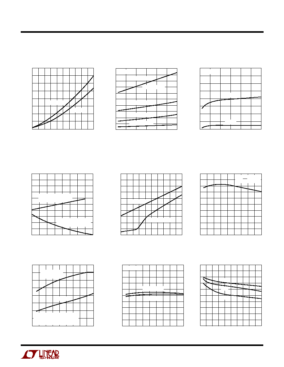
TYPICAL PERFOR
M
A
N
CE CHARACTERISTICS
U
W
Switch Current Limit vs Duty Cycle
DUTY CYCLE (%)
0
SWITCH CURRENT (A)
16
14
12
10
8
6
4
2
0
80
1070/71 G01
20
40
60
100
70
10
30
50
90
FOR LT1071, DIVIDE
VERTICAL SCALE BY 2
≠ 55
∞
C
125
∞
C
25
∞
C
Flyback Blanking Time
JUNCTION TEMPERATURE (
∞
C)
≠75
1.0
TIME (
µ
s)
1.2
1.6
1.8
2.0
≠ 25
25
50
150
1070/71 G03
1.4
≠ 50
0
75 100 125
2.2
JUNCTION TEMPERATURE (
∞
C)
≠75
90
DUTY CYCLE (%)
91
93
94
95
≠ 25
25
50
150
1070/71 G02
92
≠ 50
0
75 100 125
96
Maximum Duty Cycle
Minimum Input Voltage
TEMPERATURE (
∞
C)
≠75
2.3
MINIMUM INPUT VOLTAGE (V) 2.4
2.6
2.7
2.8
≠ 25
25
50
150
1070/71 G04
2.5
≠ 50
0
75 100 125
2.9
SWITCH CURRENT = 5A
SWITCH CURRENT = 0A
Switch Saturation Voltage
SWITCH CURRENT (A)
0
SWITCH SATURATION VOLTAGE (V)
0.8
1.2
8
1070/71 G05
0.4
0
1.0
25
∞
C
1.4
0.6
0.2
2
4
6
1
3
5
7
1.6
FOR LT1071, DIVIDE
CURRENT BY 2
100
∞
C
≠ 55
∞
C
150
∞
C
Isolated Mode Flyback
Reference Voltage
TEMPERATURE (
∞
C)
≠ 75
FLYBACK VOLTAGE (V)
19
20
21
125
1070/71 G06
18
17
15
≠ 25
25
75
≠ 50
150
0
50
100
16
23
22
R
FEEDBACK
= 500
R
FEEDBACK
= 1k
R
FEEDBACK
= 10k
Line Regulation
Feedback Bias Current
vs Temperature
INPUT VOLTAGE (V)
0
≠ 5
REFERENCE VOLTAGE CHANGE (mV)
≠ 3
≠1
1
10
20
30
40
1070/71 G07
50
3
5
≠ 4
≠ 2
0
2
4
60
T
J
= 150
∞
C
T
J
= 25
∞
C
T
J
= ≠ 55
∞
C
TEMPERATURE (
∞
C)
≠ 75
FEEDBACK BIAS CURRENT (nA)
600
500
400
300
200
100
0
125
1070/71 G09
≠ 25
25
75
≠ 50
150
0
50
100
800
700
Reference Voltage
vs Temperature
TEMPERATURE (
∞
C)
≠ 75
REFERENCE VOLTAGE (V)
SWITCHING FREQUENCY (kHz)
1.246
1.244
1.242
1.240
1.238
1.236
1.234
125
1070/71 G08
≠ 25
25
75
≠ 50
150
0
50
100
1.250
1.248
40
39
38
37
36
35
34
42
41
SWITCHING
FREQUENCY
REFERENCE
V0LTAGE
5
LT1070/LT1071
TYPICAL PERFOR
M
A
N
CE CHARACTERISTICS
U
W
Supply Current vs Supply Voltage
(Shutdown Mode)
Driver Current* vs Switch Current
SWITCH CURRENT (A)
0
DRIVER CURRENT (mA)
160
140
120
100
80
60
40
20
0
4
1070/71 G10
1
*
2
3
5
T
J
25
∞
C
AVERAGE LT1070 POWER SUPPLY CURRENT IS
FOUND BY MULTIPLYING DRIVER CURRENT BY
DUTY CYCLE, THEN ADDING QUIESCENT CURRENT
T
J
= ≠ 55
∞
C
SUPPLY VOLTAGE (V)
0
SUPPLY CURRENT (
µ
A)
60
80
100
30
50
1070/71 G12
40
20
0
10
20
40
120
140
160
60
T
J
= 25
∞
C
V
C
= 50mV
V
C
= 0V
Supply Current vs Input Voltage*
INPUT VOLTAGE (V)
0
6
INPUT CURRENT (mA)
8
10
12
10
20
30
*
40
1070/71 G11
50
14
UNDER VERY LOW OUTPUT CURRENT
CONDITIONS, DUTY CYCLE FOR MOST
CIRCUITS WILL APPROACH 10% OR LESS
16
7
9
11
13
15
60
T
J
= 25
∞
C
I
SWITCH
10mA
90% DUTY CYCLE
50% DUTY CYCLE
0% DUTY CYCLE
10% DUTY CYCLE
Feedback Pin Clamp Voltage
Shutdown Thresholds
TEMPERATURE (
∞
C)
≠ 75
V
C
PIN VOLTAGE (mV)
V
C
PIN CURRENT (
µ
A)
300
250
200
150
100
50
0
125
1070/71 G16
≠ 25
25
75
≠ 50
150
0
50
100
400
350
≠300
≠250
≠200
≠150
≠100
≠ 50
0
≠ 400
≠350
V
C
VOLTAGE IS REDUCED UNTIL
REGULATOR CURRENT DROPS
BELOW 300
µ
A
VOLTAGE
CURRENT
(OUT OF V
C
PIN)
FEEDBACK CURRENT (mA)
0
FEEDBACK VOLTAGE (mV)
300
400
500
0.8
1070/71 G18
200
100
250
350
450
150
50
0
0.2
0.4
0.6
0.1
0.9
0.3
0.5
0.7
1.0
≠ 55
∞
C
25
∞
C
150
∞
C
TEMPERATURE (
∞
C)
≠75
IDLE SUPPLY CURRENT (mA)
7
9
11
125
1070/71 G14
5
3
6
8
10
4
2
1
≠25
25
75
≠ 50
150
0
50
100
V
C
= 0.6V
V
SUPPLY
= 60V
V
SUPPLY
= 3V
Idle Supply Current
vs Temperature
Normal/Flyback Mode Threshold
on Feedback Pin
TEMPERATURE (
∞
C)
≠50
400
FEEDBACK PIN VOLTAGE (mV)
FEEDBACK PIN CURRENT (
µ
A)
410
430
440
450
500
470
0
50
75
1070/71 G13
420
480
490
460
≠ 4
≠ 6
≠10
≠12
≠14
≠24
≠18
≠ 8
≠20
≠22
≠16
≠25
25
100 125
150
FEEDBACK PIN VOLTAGE
(AT THRESHOLD)
FEEDBACK PIN CURRENT
(AT THRESHOLD)
Error Amplifier Transconductance
TEMPERATURE (
∞
C)
≠75
TRANSCONDUCTANCE (
µ
mho)
3000
4000
5000
125
1070/71 G14
2000
1000
2500
3500
4500
1500
500
0
≠25
25
75
≠ 50
150
0
50
100
g
m
=
(V
C
PIN)
(FB PIN)
I
V
Shutdown Mode Supply Current
V
C
PIN VOLTAGE (mV)
0
SUPPLY CURRENT (
µ
A)
120
160
200
80
1070/71 G14
80
40
100
140
180
60
20
0
20
40
60
10
90
30
50
70
100
T
J
= 150
∞
C
≠ 55
∞
C
T
J
125
∞
C