 | –≠–ª–µ–∫—Ç—Ä–æ–Ω–Ω—ã–π –∫–æ–º–ø–æ–Ω–µ–Ω—Ç: LT1113CN8 | –°–∫–∞—á–∞—Ç—å:  PDF PDF  ZIP ZIP |

1
LT1113
The LT
Æ
1113 achieves a new standard of excellence in noise
performance for a dual JFET op amp. The 4.5nV/
Hz 1kHz
noise combined with low current noise and picoampere
bias currents makes the LT1113 an ideal choice for ampli-
fying low level signals from high impedance capacitive
transducers.
The LT1113 is unconditionally stable for gains of 1 or more,
even with load capacitances up to 1000pF. Other key fea-
tures are 0.4mV V
OS
and a voltage gain of 4 million. Each
individual amplifier is 100% tested for voltage noise, slew
rate and gain bandwidth.
The design of the LT1113 has been optimized to achieve
true precision performance with an industry standard
pinout in the S0-8 package. A set of specifications are
provided for
±
5V supplies and a full set of matching speci-
fications are provided to facilitate the use of the LT1113 in
matching dependent applications such as instrumenta-
tion amplifier front ends.
Dual Low Noise,
Precision, JFET Input Op Amps
s
100% Tested Low Voltage Noise: 6nV/
Hz Max
s
SO-8 Package Standard Pinout
s
Voltage Gain: 1.2 Million Min
s
Offset Voltage: 1.5mV Max
s
Offset Voltage Drift: 15
µ
V/
∞
C Max
s
Input Bias Current, Warmed Up: 450pA Max
s
Gain Bandwidth Product: 5.6MHz Typ
s
Guaranteed Specifications with
±
5V Supplies
s
Guaranteed Matching Specifications
s
Photocurrent Amplifiers
s
Hydrophone Amplifiers
s
High Sensitivity Piezoelectric Accelerometers
s
Low Voltage and Current Noise Instrumentation
Amplifier Front Ends
s
Two and Three Op Amp Instrumentation Amplifiers
s
Active Filters
Low Noise Hydrophone Amplifier with DC Servo
1kHz Input Noise Voltage Distribution
FEATURES
DESCRIPTIO
U
APPLICATIO S
U
TYPICAL APPLICATIO
U
, LTC and LT are registered trademarks of Linear Technology Corporation.
≠
+
≠
+
8
4
5V TO 15V
1
2
3
≠5V TO ≠15V
C2
0.47
µ
F
6
5
7
R8
100M
R6
100k
R4
1M
R5
1M
1/2
LT1113
1/2
LT1113
R3
3.9k
C1*
R1*
100M
R7
1M
R2
200
C
T
HYDRO-
PHONE
OUTPUT
DC OUTPUT
2.5mV FOR T
A
< 70
∞
C
OUTPUT VOLTAGE NOISE = 128nV/
Hz AT 1kHz (GAIN = 20)
C1
C
T
100pF TO 5000pF; R4C2 > R8C
T
; *OPTIONAL
1113 TA01
INPUT VOLTAGE NOISE (nV/
Hz)
3.8
PERCENT OF UNITS (%)
40
30
20
10
0
4.2
4.6 4.8
5.8
1113 TA02
4.0
4.4
5.0 5.2 5.4 5.6
V
S
=
±
15V
T
A
= 25
∞
C
138 S8
276 OP AMPS TESTED
2
LT1113
A
U
G
W
A
W
U
W
A
R
BSOLUTE
XI
TI
S
W
U
U
PACKAGE/ORDER I FOR ATIO
Supply Voltage
≠55
∞
C to 105
∞
C ...............................................
±
20V
105
∞
C to 125
∞
C ...............................................
±
16V
Differential Input Voltage ......................................
±
40V
Input Voltage (Equal to Supply Voltage) ...............
±
20V
Output Short Circuit Duration .......................... 1 Minute
Storage Temperature Range ................ ≠ 65
∞
C to 150
∞
C
Operating Temperature Range
LT1113AC/LT1113C (Note 2) .......... ≠ 40
∞
C to 85
∞
C
LT1113AM/LT1113M .................... ≠ 55
∞
C to 125
∞
C
Specified Temperature Range
LT1113AC/LT1113C (Note 3) .......... ≠ 40
∞
C to 85
∞
C
LT1113AM/LT1113M .................... ≠ 55
∞
C to 125
∞
C
Lead Temperature (Soldering, 10 sec) ................ 300
∞
C
ELECTRICAL C
C
HARA TERISTICS
LT1113CS8
S8 PART MARKING
1113
LT1113AMJ8
LT1113MJ8
LT1113ACN8
LT1113CN8
T
JMAX
= 150
∞
C,
JA
= 190
∞
C/W
T
JMAX
= 160
∞
C,
JA
= 100
∞
C/W (J8)
T
JMAX
= 150
∞
C,
JA
= 130
∞
C/W (N8)
LT1113AM/AC
LT1113M/C
SYMBOL PARAMETER
CONDITIONS (Note 4)
MIN
TYP
MAX
MIN
TYP
MAX
UNITS
V
OS
Input Offset Voltage
0.40
1.5
0.50
1.8
mV
V
S
=
±
5V
0.45
1.7
0.55
2.0
mV
I
OS
Input Offset Current
Warmed Up (Note 5)
30
100
35
150
pA
I
B
Input Bias Current
Warmed Up (Note 5)
300
450
320
480
pA
e
n
Input Noise Voltage
0.1Hz to 10Hz
2.4
2.4
µ
V
P-P
Input Noise Voltage Density
f
O
= 10Hz
17
17
nV/
Hz
f
O
= 1000Hz
4.5
6.0
4.5
6.0
nV/
Hz
i
n
Input Noise Current Density
f
O
= 10Hz, f
O
= 1000Hz (Note 6)
10
10
fA/
Hz
R
IN
Input Resistance
Differential Mode
10
11
10
11
Common Mode
V
CM
= ≠ 10V to 8V
10
11
10
11
V
CM
= 8V to 11V
10
10
10
10
C
IN
Input Capacitance
14
14
pF
V
S
=
±
5V
27
27
pF
V
CM
Input Voltage Range (Note 7)
13.0
13.5
13.0
13.5
V
≠10.5
≠11.0
≠10.5
≠11.0
V
CMRR
Common Mode Rejection Ratio V
CM
= ≠10V to 13V
85
98
82
95
dB
PSRR
Power Supply Rejection Ratio
V
S
=
±
4.5V to
±
20V
86
100
83
98
dB
A
VOL
Large-Signal Voltage Gain
V
O
=
±
12V, R
L
= 10k
1200
4800
1000
4500
V/mV
V
O
=
±
10V, R
L
= 1k
600
4000
500
3000
V/mV
V
S
=
±
15V, V
CM
= 0V, T
A
= 25
∞
C, unless otherwise noted.
ORDER PART
NUMBER
ORDER PART
NUMBER
(Note 1)
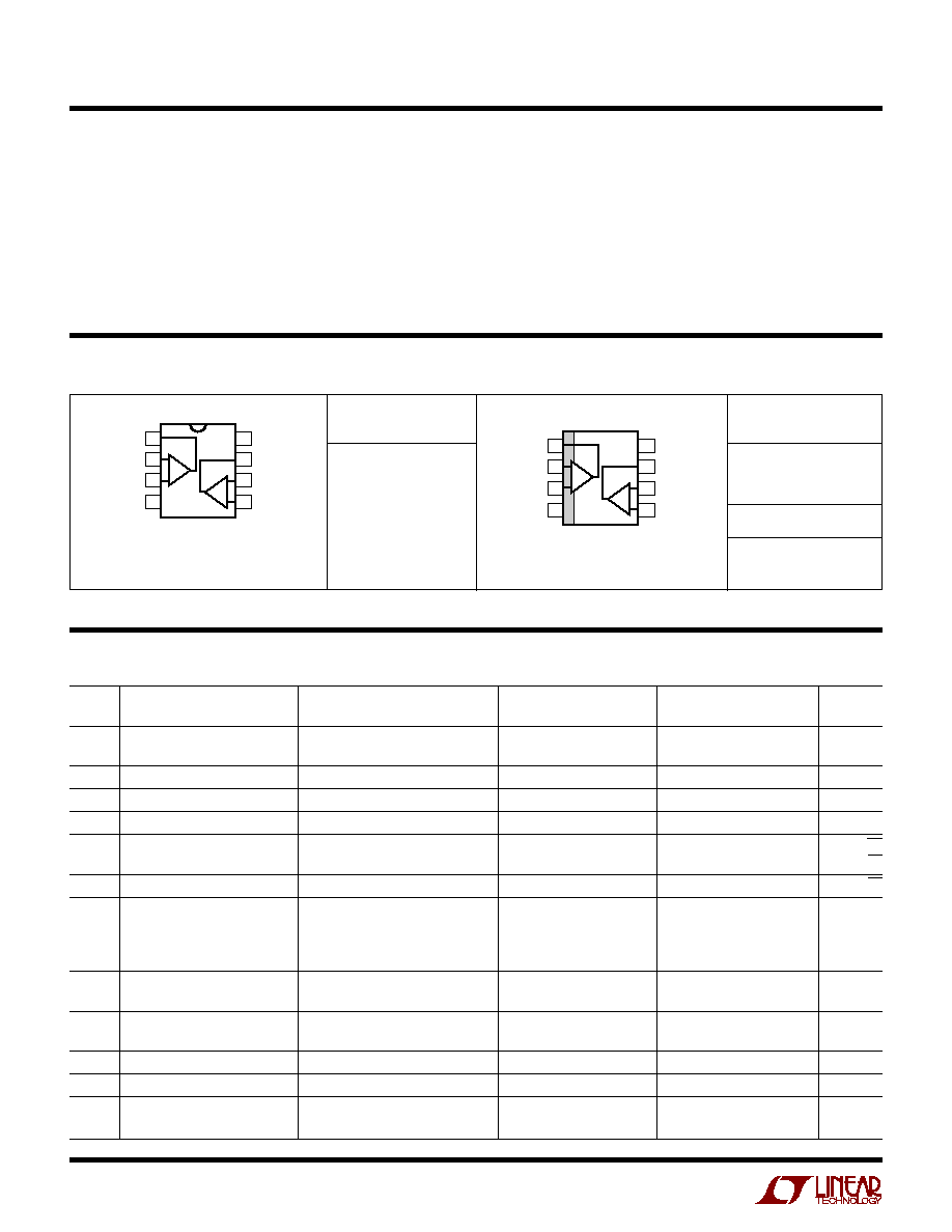
1
2
3
4
8
7
6
5
TOP VIEW
N8 PACKAGE
8-LEAD PDIP
J8 PACKAGE
8-LEAD CERDIP
B
A
OUT A
≠IN A
+IN A
V
≠
V
+
OUT B
≠IN B
+IN B
1
2
3
4
8
7
6
5
TOP VIEW
S8 PACKAGE
8-LEAD PLASTIC SO
B
A
OUT A
≠IN A
+IN A
V
≠
V
+
OUT B
≠IN B
+IN B
Consult factory for Industrial grade parts.
3
LT1113
ELECTRICAL C
C
HARA TERISTICS
LT1113AM/AC
LT1113M/C
SYMBOL PARAMETER
CONDITIONS
MIN
TYP
MAX
MIN
TYP
MAX
UNITS
V
OUT
Output Voltage Swing
R
L
= 10k
±
13.5
±
13.8
±
13.0
±
13.8
V
R
L
= 1k
±
12.0
±
13.0
±
11.5
±
13.0
V
SR
Slew Rate
R
L
2k (Note 9)
2.3
3.9
2.3
3.9
V/
µ
s
GBW
Gain Bandwidth Product
f
O
= 100kHz
4.0
5.6
4.0
5.6
MHz
t
S
Settling Time
0.01%, A
V
= + 1, R
L
= 1k,
4.2
4.2
µ
s
C
L
1000pF, 10V Step
Channel Separation
f
O
= 10Hz, V
O
=
±
10V, R
L
= 1k
130
126
dB
I
S
Supply Current per Amplifier
5.3
6.25
5.3
6.50
mA
V
S
=
±
5V
5.3
6.20
5.3
6.45
mA
V
OS
Offset Voltage Match
0.8
2.5
0.8
3.3
mV
I
B
+
Noninverting Bias Current Match
Warmed Up (Note 5)
10
80
10
120
pA
CMRR
Common Mode Rejection Match (Note 11)
81
94
78
94
dB
PSRR
Power Supply Rejection Match
(Note 11)
82
95
80
95
dB
LT1113AC
LT1113C
SYMBOL PARAMETER
CONDITIONS (Note 4)
MIN
TYP
MAX
MIN
TYP
MAX
UNITS
V
OS
Input Offset Voltage
q
0.6
2.1
0.7
2.5
mV
V
S
=
±
5V
q
0.7
2.3
0.8
2.7
mV
V
OS
Average Input Offset
(Note 8)
q
7
15
8
20
µ
V/
∞
C
Temp
Voltage Drift
I
OS
Input Offset Current
q
50
350
55
450
pA
I
B
Input Bias Current
q
600
1200
700
1600
pA
V
CM
Input Voltage Range
q
12.9
13.4
12.9
13.4
V
q
≠10.0
≠10.8
≠10.0
≠10.8
V
CMRR
Common Mode Rejection Ratio
V
CM
= ≠10V to 12.9V
q
81
97
79
94
dB
PSRR
Power Supply Rejection Ratio
V
S
=
±
4.5V to
±
20V
q
83
99
81
97
dB
A
VOL
Large-Signal Voltage Gain
V
O
=
±
12V, R
L
= 10k
q
900
3600
800
3400
V/mV
V
O
=
±
10V, R
L
= 1k
q
500
2600
400
2400
V/mV
V
OUT
Output Voltage Swing
R
L
= 10k
q
±
13.2
±
13.5
±
12.7
±
13.5
V
R
L
= 1k
q
±
11.7
±
12.7
±
11.3
±
12.7
V
SR
Slew Rate
R
L
2k
(Note 9)
q
2.1
3.7
1.7
3.7
V/
µ
s
GBW
Gain Bandwidth Product
f
O
= 100kHz
q
3.2
4.5
3.2
4.5
MHz
I
S
Supply Current per Amplifier
q
5.3
6.35
5.3
6.55
mA
V
S
=
±
5V
q
5.3
6.30
5.3
6.50
mA
V
OS
Offset Voltage Match
q
0.9
3.5
0.9
4.5
mV
I
B
+
Noninverting Bias Current Match
q
30
300
35
400
pA
CMRR
Common Mode Rejection Match (Note 11)
q
76
93
74
93
dB
PSRR
Power Supply Rejection Match
(Note 11)
q
79
93
77
93
dB
V
S
=
±
15V, V
CM
= 0V, T
A
= 25
∞
C, unless otherwise noted.
The
q
denotes specifications which apply over the temperature range 0
∞
C
T
A
70
∞
C. V
S
=
±
15V, V
CM
= 0V,
unless otherwise noted. (Note 12)
4
LT1113
LT1113AC
LT1113C
SYMBOL PARAMETER
CONDITIONS (Note 4)
MIN
TYP
MAX
MIN
TYP
MAX
UNITS
V
OS
Input Offset Voltage
q
0.7
2.4
0.8
2.8
mV
V
S
=
±
5V
q
0.8
2.6
0.9
3.0
mV
V
OS
Average Input Offset
q
7
15
8
20
µ
V/
∞
C
Temp
Voltage Drift
I
OS
Input Offset Current
q
80
700
90
1000
pA
I
B
Input Bias Current
q
1750
3000
1800
5000
pA
V
CM
Input Voltage Range
q
12.6
13.0
12.6
13.0
V
q
≠10.0
≠10.5
≠10.0
≠10.5
V
CMRR
Common Mode Rejection Ratio
V
CM
= ≠10V to 12.6V
q
80
96
78
93
dB
PSRR
Power Supply Rejection Ratio
V
S
=
±
4.5V to
±
20V
q
81
98
79
96
dB
A
VOL
Large-Signal Voltage Gain
V
O
=
±
12V, R
L
= 10k
q
850
3300
750
3000
V/mV
V
O
=
±
10V, R
L
= 1k
q
400
2200
300
2000
V/mV
V
OUT
Output Voltage Swing
R
L
= 10k
q
±
13.0
±
12.5
±
12.5
±
12.5
V
R
L
= 1k
q
±
11.5
±
12.0
±
11.0
±
12.0
V
SR
Slew Rate
R
L
2k
q
2.0
3.5
1.6
3.5
V/
µ
s
GBW
Gain Bandwidth Product
f
O
= 100kHz
q
2.9
4.3
2.9
4.3
MHz
I
S
Supply Current per Amplifier
q
5.30
6.35
5.30
6.55
mA
V
S
=
±
5V
q
5.25
6.30
5.25
6.50
mA
V
OS
Offset Voltage Match
q
1.0
4.4
1.0
5.1
mV
I
B
+
Noninverting Bias Current Match
q
50
600
55
900
pA
CMRR
Common Mode Rejection Match (Note 11)
q
76
93
73
93
dB
PSRR
Power Supply Rejection Match
(Note 11)
q
77
92
75
92
dB
ELECTRICAL C
C
HARA TERISTICS
LT1113AM
LT1113M
SYMBOL PARAMETER
CONDITIONS (Note 4)
MIN
TYP
MAX
MIN
TYP
MAX
UNITS
V
OS
Input Offset Voltage
q
0.8
2.7
0.9
3.3
mV
V
S
=
±
5V
q
0.8
2.8
0.9
3.4
mV
V
OS
Average Input Offset
(Note 8)
q
5
12
8
15
µ
V/
∞
C
Temp
Voltage Drift
I
OS
Input Offset Current
q
0.8
15
1.0
25
nA
I
B
Input Bias Current
q
25
50
27
70
nA
V
CM
Input Voltage Range
q
12.6
13.0
12.6
13.0
V
q
≠10.0
≠10.4
≠10.0
≠10.4
V
CMRR
Common Mode Rejection Ratio
V
CM
= ≠10V to 12.6V
q
79
95
77
92
dB
PSRR
Power Supply Rejection Ratio
V
S
=
±
4.5V to
±
20V
q
80
97
78
95
dB
The
q
denotes specifications which apply over the temperature range ≠40
∞
C
T
A
85
∞
C. V
S
=
±
15V, V
CM
= 0V,
unless otherwise noted. (Note 10)
The
q
denotes specifications which apply over the temperature range ≠55
∞
C
T
A
125
∞
C. V
S
=
±
15V, V
CM
= 0V,
unless otherwise noted. (Note 12)
5
LT1113
ELECTRICAL C
C
HARA TERISTICS
LT1113AM
LT1113M
SYMBOL PARAMETER
CONDITIONS (Note 4)
MIN
TYP
MAX
MIN
TYP
MAX
UNITS
A
VOL
Large-Signal Voltage Gain
V
O
=
±
12V, R
L
= 10k
q
800
2700
700
2500
V/mV
V
O
=
±
10V, R
L
= 1k
q
400
1500
300
1000
V/mV
V
OUT
Output Voltage Swing
R
L
= 10k
q
±
13.0
±
12.5
±
12.5
±
12.5
V
R
L
= 1k
q
±
11.5
±
12.0
±
11.0
±
12.0
V
SR
Slew Rate
R
L
2k
(Note 9)
q
1.9
3.3
1.6
3.3
V/
µ
s
GBW
Gain Bandwidth Product
f
O
= 100kHz
q
2.2
3.4
2.2
3.4
MHz
I
S
Supply Current Per Amplifier
q
5.30
6.35
5.30
6.55
mA
V
S
=
±
5V
q
5.25
6.30
5.25
6.50
mA
V
OS
Offset Voltage Match
q
1.0
5.0
1.0
5.5
mV
I
B
+
Noninverting Bias Current Match
q
1.8
12
2.0
20
nA
CMRR
Common Mode Rejection Match (Note 11)
q
75
92
73
92
dB
PSRR
Power Supply Rejection Match
(Note 11)
q
76
91
74
91
dB
The
q
denotes specifications which apply over the temperature range ≠ 55
∞
C
T
A
125
∞
C.
V
S
=
±
15V, V
CM
= 0V,
unless otherwise noted. (Note 12)
Note 1: Absolute Maximum Ratings are those values beyond which the
life of the device may be impaired.
Note 2: The LT1113C is guaranteed functional over the Operating
Temperature Range of ≠40
∞
C to 85
∞
C. The LT1113M is guaranteed
functional over the Operating Temperature Range of ≠ 55
∞
C to 125
∞
C.
Note 3: The LT1113C is guaranteed to meet specified performance from
0
∞
C to 70
∞
C. The LT1113C is designed, characterized and expected to
meet specified performance from ≠40
∞
C to 85
∞
C but is not tested or QA
sampled at these temperatures. For guaranteed I grade parts, consult the
factory. The LT1113M is guaranteed to meet specified performance from
≠55
∞
C to 125
∞
C.
Note 4: Typical parameters are defined as the 60% yield of parameter
distributions of individual amplifiers, i.e., out of 100 LT1113s (200 op
amps) typically 120 op amps will be better than the indicated
specification.
Note 5: Warmed-up I
B
and I
OS
readings are extrapolated to a chip
temperature of 50
∞
C from 25
∞
C measurements and 50
∞
C characterization
data.
Note 6: Current noise is calculated from the formula:
i
n
= (2qI
B
)
1/2
where q = 1.6 ∑ 10
≠19
coulomb. The noise of source resistors up to 200M
swamps the contribution of current noise.
Note 7: Input voltage range functionality is assured by testing offset
voltage at the input voltage range limits to a maximum of 2.3mV
(A grade) to 2.8mV (C grade).
Note 8: This parameter is not 100% tested.
Note 9: Slew rate is measured in A
V
= ≠1; input signal is
±
7.5V, output
measured at
±
2.5V.
Note 10: The LT1113 is designed, characterized and expected to meet
these extended temperature limits, but is not tested at ≠40
∞
C and 85
∞
C.
Guaranteed I grade parts are available. Consult factory.
Note 11:
CMRR and
PSRR are defined as follows:
(1) CMRR and PSRR are measured in
µ
V/ V on the individual
amplifiers.
(2) The difference is calculated between the matching sides in
µ
V/ V.
(3) The result is converted to dB.
Note 12: The LT1113 is measured in an automated tester in less than
one second after application of power. Depending on the package used,
power dissipation, heat sinking, and air flow conditions, the fully
warmed-up chip temperature can be 10
∞
C to 50
∞
C higher than the
ambient temperature.