 | –≠–ª–µ–∫—Ç—Ä–æ–Ω–Ω—ã–π –∫–æ–º–ø–æ–Ω–µ–Ω—Ç: LT1118CS8 | –°–∫–∞—á–∞—Ç—å:  PDF PDF  ZIP ZIP |
1
LT1118/LT1118-2.5
LT1118-2.85/LT1118-5
Low I
Q
, Low Dropout,
800mA, Source and Sink
Regulators Adjustable and
Fixed 2.5V, 2.85V, 5V Output
FEATURES
APPLICATIO
N
S
U
TYPICAL APPLICATIO
N
U
, LTC and LT are registered trademarks of Linear Technology Corporation.
The LT
Æ
1118 family of low dropout regulators has the
unique capability of maintaining output regulation while
sourcing or sinking load current. The 2.85V output voltage
regulator is ideal for use as a Boulay termination of up to
27 SCSI data lines. The regulator maintains regulation
while both sourcing and sinking current, enabling the use
of active negation drivers for improved noise immunity on
the data lines. Regulation of output voltage is maintained
for TERMPWR voltages as low as 4.0V. When unloaded,
quiescent supply current is a low 600
µ
A, allowing continu-
ous connection to the TERMPWR lines. An ultralow power
shutdown mode is also available on the SO-8 version. In
Shutdown the output is high impedance and supply cur-
rent drops to less than 10
µ
A.
Current limits in both sourcing and sinking modes, plus
on-chip thermal shutdown make the circuit tolerant of
output fault conditions.
The LT1118 is available in 3-lead SOT-223 and 8-lead SO
packages.
s
Active Negation SCSI Terminations
s
Computers
s
Disk Drives
s
CD-ROM
s
Supply Splitter
s
Regulates While Sourcing or Sinking Current
s
Provides Termination for up to 27 SCSI Lines
s
600
µ
A Quiescent Current
s
Ultra-Low Power Shutdown Mode
s
Current Limit and Thermal Shutdown Protection
s
Stable for Any C
LOAD
0.22
µ
F
s
Fast Settling Time
s
1V Dropout Voltage
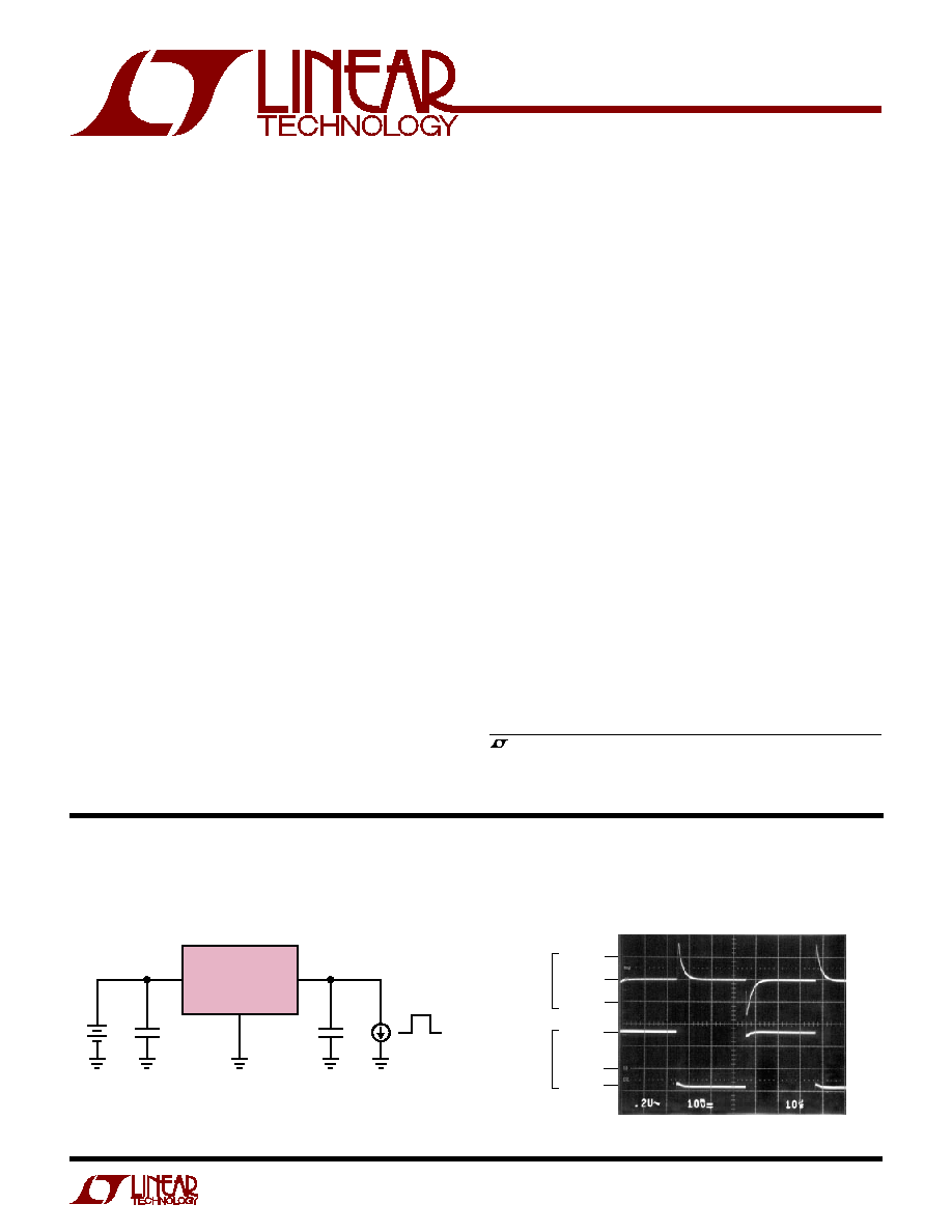
Load Transient Response
1118 TA02.tif
0.2V
0V
≠ 0.2V
LT1118-2.85
GND
1118 TA01
IN
2.2
µ
F
5V
1
µ
F
CERAMIC
I
LOAD
OUT
I
LOAD
≠ 400mA
800mA
0mA
V
OUT
DESCRIPTIO
N
U

2
LT1118/LT1118-2.5
LT1118-2.85/LT1118-5
ABSOLUTE
M
AXI
M
U
M
RATINGS
W
W
W
U
PACKAGE/ORDER I
N
FOR
M
ATIO
N
W
U
U
Consult factory for Industrial and Military grade parts.
1118
S8 PART MARKING
111825
111828
11185
S8 PART MARKING
T
JMAX
= 125
∞
C,
JC
= 15
∞
C/W
T
JMAX
= 125
∞
C,
JC
= 15
∞
C/W
T
JMAX
= 125
∞
C,
JC
= 15
∞
C/W
ORDER PART NUMBER
ORDER PART NUMBER
ORDER PART NUMBER
LT1118CS8-2.5
LT1118CS8-2.85
LT1118CS8-5
LT1118CST-2.5
LT1118CST-2.85
LT1118CST-5
LT1118CS8
1
2
3
4
8
7
6
5
TOP VIEW
S8 PACKAGE
8-LEAD PLASTIC SO
GND
IN
OUT
IN
GND
NC
EN
FB
1
2
3
4
8
7
6
5
TOP VIEW
S8 PACKAGE
8-LEAD PLASTIC SO
EN
GND
GND
NC
IN
OUT
GND
IN
3
2
1
FRONT VIEW
TAB IS
GND
IN
GND
OUT
ST PACKAGE
3-LEAD PLASTIC SOT-223
Operating Temperature Range ..................... 0
∞
C to 70
∞
C
Storage Temperature Range ................. ≠ 65
∞
C to 150
∞
C
Lead Temperature (Soldering, 10 sec).................. 300
∞
C
Supply Voltage (V
CC
) ............................................... 15V
Input Voltage (Enable) ................................ ≠ 0.2V to 7V
Output Voltage ................................ ≠ 0.2V to V
CC
+ 0.5V
Short-Circuit Duration ..................................... Indefinite
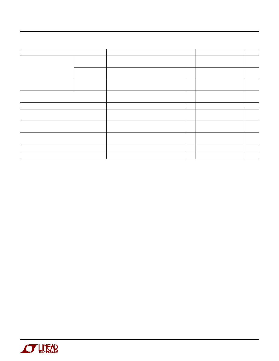
PARAMETER
CONDITIONS
MIN
TYP
MAX
UNITS
Quiescent Current (V
IN
)
V
EN
= 5V
q
0.6
1
mA
Quiescent Current in Shutdown (V
IN
)
V
EN
= 0V
q
1
10
µ
A
Enable Input Thresholds
Input Low Level
q
0.4
1.4
V
Input High Level
q
1.4
2
V
Enable Input Current
0V
V
EN
5V
q
≠1
25
µ
A
Output Voltage
LT1118-2.5
No Load (25
∞
C)
2.47
2.5
2.53
V
All Operating Conditions (Note 3)
q
2.45
2.5
2.55
V
LT1118-2.85
No Load (25
∞
C)
2.82
2.85
2.88
V
All Operating Conditions (Note 3)
q
2.79
2.85
2.91
V
LT1118-5
No Load (25
∞
C)
4.95
5
5.05
V
All Operating Conditions (Note 3)
q
4.90
5
5.1
V
Line Regulation (Note 4)
LT1118-2.5
I
L
= 0mA, 4.2V
V
IN
15V
q
6
mV
LT1118-2.85
I
L
= 0mA, 4.75V
V
IN
15V
q
6
mV
LT1118-5
I
L
= 0mA, 6.5V
V
IN
15V
q
10
mV
ELECTRICAL CHARACTERISTICS
(Note 1)
(Note 2)
3
LT1118/LT1118-2.5
LT1118-2.85/LT1118-5
ELECTRICAL CHARACTERISTICS
PARAMETER
CONDITIONS
MIN
TYP
MAX
UNITS
Load Regulation (Note 4)
LT1118-2.5
0mA
I
L
800mA
q
10
mV
≠ 400mA
I
L
0mA
q
10
mV
LT1118-2.85
0mA
I
L
800mA
q
10
mV
≠ 400mA
I
L
0mA
q
10
mV
LT1118-5
0mA
I
L
800mA
q
20
mV
≠ 400mA
I
L
0mA
q
20
mV
Dropout Voltage (Note 5)
I
L
= 100mA
0.85
1.1
V
I
L
= 800mA
1
1.3
V
Minimum Output Voltage
LT1118
q
2
V
Ripple Rejection
f
RIPPLE
= 120Hz, V
IN
≠ V
OUT
= 2V
60
80
dB
V
RIPPLE
= 0.5V
P-P
Load Transient Settling Time,
0mA
I
L
800mA, C
LOAD
= 1
µ
F
5
µ
s
V = 1%
≠ 400mA
I
L
0mA, C
LOAD
= 1
µ
F
5
µ
s
Output Short-Circuit Current
I
SC
+
V
OUT
= 0V
800
1200
mA
I
SC
≠
V
OUT
= V
IN
≠ 700
≠ 400
mA
Thermal Shutdown Junction Temperature
No Load
170
∞
C
Enable Turn-On Delay
No Load
50
µ
s
The
q
denotes specifications which apply over the operating temperature
range.
Note 1: Absolute maximum ratings are those values beyond which the life
of the device may be impaired.
Note 2: Unless otherwide specified, testing done at V
CC
= 5V
(LT1118-2.5, LT1118-2.85) or V
CC
= 7V (LT1118-5). V
EN
= V
CC
. Output
C
LOAD
= 1
µ
F, I
LOAD
= 0.
Note 3: All operating conditions include the combined effects of load
current, input voltage and temperature over each parameter's full range.
Note 4: Load and line regulation are tested at a constant junction
temperature by low duty cycle pulse testing.
Note 5: Dropout voltage is defined as the minimum input to output voltage
measured while sourcing the specified current.
(Note 2)

4
LT1118/LT1118-2.5
LT1118-2.85/LT1118-5
TYPICAL PERFOR
M
A
N
CE CHARACTERISTICS
U
W
Output Impedance vs Frequency
Ripple Rejection vs Load Current
Feedback Current vs Temperature
FREQUENCY (Hz)
10
2
0.001
Z
OUT
(mA)
0.1
10
10
4
10
5
10
3
10
6
1118 G04
0.01
1
NO CURRENT
10mA SOURCE
100mA SOURCE
10mA SINK
100mA SINK
OUTPUT SINK CURRENT (mA)
0
INPUT CURRENT (
µ
A)
1000
1250
1500
400
1118 G07
750
500
0
100
200
300
250
2000
1750
50
150
250
350
OUTPUT SOURCING CURRENT (mA)
0
GROUND PIN CURRENT (
µ
A)
400
500
600
800
1118 G08
300
200
0
200
400
600
100
800
700
TEMP
≠55 ≠35 ≠15
5
25
45
65
85 105 125
CURRENT (nA)
450
400
350
300
250
200
150
100
50
0
1118 G05
LOAD CURRENT (mA)
≠400
RIPPLE REJECTION (dB)
80
60
40
20
0
≠200
0
200
400
1118 G06
600
800
C
IN
= C
LOAD
= 1
µ
F
Input Current vs
Output Sink Current
Ground Pin Current vs
Output Source Current
Dropout Voltage vs Output Current
Ripple Rejection vs Frequency
Ripple Rejection vs Frequency
OUTPUT CURRENT (mA)
0
200
400
600
800
DROPOUT VOLTAGE
1118 G01
1.4
1.2
1
0.8
0.6
0.4
0.2
0
T
J
= 75
∞
C
T
J
= 25
∞
C
T
J
= 125
∞
C
FREQUENCY (Hz)
RIPPLE REJECTION (dB)
80
60
40
20
0
10
1k
10k
100k
1118 G02
100
SOURCING CURRENT
NO LOAD
800mA
10mA
FREQUENCY (Hz)
RIPPLE REJECTION (dB)
80
60
40
20
0
10
1k
10k
100k
1118 G03
100
SINKING CURRENT
NO LOAD
400mA
10mA

5
LT1118/LT1118-2.5
LT1118-2.85/LT1118-5
PI
N
FU
N
CTIO
N
S
U
U
U
IN: Input Supply Pin. This pin should be decoupled with a
1
µ
F or larger low ESR capacitor. The two IN pins on the
SO-8 package must be directly connected on the printed
circuit board to prevent voltage drops between the two
inputs. When used as a SCSI active termination, IN con-
nects to term power. When used as a supply splitter, IN is
also the positive supply output.
GND: Ground Pin. The multiple GND pins on the SO-8
package are internally connected, but lowest load regula-
tion errors will result if these pins are tightly connected on
the printed circuit board. This will also aid heat dissipation
at high power levels.
EN: TTL/CMOS Logic Input. A high level allows normal
operation. A low level reduces supply current to zero. This
pin is internally connected to V
IN
on 3-lead ST packaged
devices.
OUT: Regulated Output Voltage. Output can source or sink
current. Current limit for sourcing and sinking current is
provided to protect the device from fault conditons. The
output must have a low ESR output filter capacitor. C
OUT
0.22
µ
F to guarantee stability. A 0.1
µ
F ceramic capacitor
may be needed in parallel with C
OUT
if the ESR of the main
C
OUT
is too high.
FB: Feedback Pin. The feedback pin is used to program the
output voltage of the adjustable S8 part. The output
voltage is determined by the selection of feedback resis-
tors defined by the following formula:
V
OUT
= V
FB
(1 + R
1
/R
2
) + I
FB
R
1
LT1118 Adjustable
GND
IN
OUT
EN
FB
R
1
R
2
1
µ
F
V
IN
1118 TA06
LT1118
1
µ
F
R
1
R
2
1 +
V
OUT
= V
FB
+ I
FB
R
1
( )
OPERATIO
U
Output Capacitor
The LT1118 family of voltage regulators require an output
capacitor for stability. The regulators are stable with
output capacitors larger than 0.2
µ
F. Load transient re-
sponse is very sensitive to output capacitor value and
dielectric choice. Low ESR ceramic capacitors are the best
choice for fast settling to load transients. Output capaci-
tors between 0.2
µ
F and 1
µ
F give good performance in
most applications. Larger tantalum output capacitors may
be used to reduce load transient amplitudes. Larger ca-
pacitors should be paralleled with a 0.1
µ
F ceramic capaci-
tor to maintain quick settling time performance and to
insure stability of the regulator control loop. Capacitors
larger than 10
µ
F may be safely used with the regulators,
but little transient settling performance improvement re-
sults from their use.
Worst case transient response of the LT1118 regulators
occurs at zero output current. In order to obtain the fastest
transient settling performance, the regulator output may
be preloaded with a small current. The preload current
reduces the regulator output impedance, reducing output
voltage settling time.
Thermal Considerations
The LT1118 regulators are packaged in plastic SOT-223
and fused lead S8 packages. These small footprint pack-
ages are unable to convectively dissipate the heat gener-
ated when the regulator is operating at high current levels.
In order to control die operating temperatures, the PC
board layout should allow for maximum possible copper
area at the ground pins of the LT1118. The ground pins
and the tab on the SOT-223 package are electrically and