 | –≠–ª–µ–∫—Ç—Ä–æ–Ω–Ω—ã–π –∫–æ–º–ø–æ–Ω–µ–Ω—Ç: LT1120A | –°–∫–∞—á–∞—Ç—å:  PDF PDF  ZIP ZIP |
1
LT1120A
s
20
µ
A Supply Current
s
8-Lead SOIC
s
125mA Output Current
s
2.5V Reference
s
Reference Output Sources 4mA and Sinks 4mA
s
Open Collector
s
Comparator Sinks 10mA
s
Logic Shutdown
s
0.2V Dropout Voltage
s
Thermal Limiting
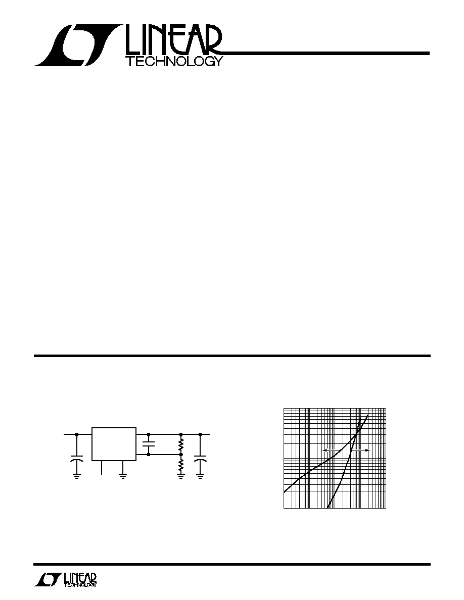
The LT1120A is a combination micropower positive regu-
lator and free collector comparator on a single monolithic
chip. With only 20
µ
A supply current, the LT1120A can
supply over 125mA of output current. Input voltage range
is from 4.5V to 36V and dropout voltage is 0.6V at 125mA.
Dropout voltage decreases with lower load currents. Also
included on the chip is a class B output 2.5V reference that
can either source or sink current. This allows it to be used
as a supply splitter or auxiliary output. A shutdown pin
allows logic shutdown of the output.
The comparator can be used for system or battery moni-
toring. For example, the comparator can be used to warn
of low system voltage. Frequency compensation of the
comparator for amplifier applications can be obtained by
adding external output capacitance.
s
Battery Systems
s
Battery Backup System
s
Portable Terminals
s
Portable Instruments
s
Memory Keep Alive
Micropower Regulator with
Comparator and Shutdown
FEATURES
DESCRIPTIO
N
U
APPLICATIO
N
S
U
TYPICAL APPLICATIO
N
U
Dropout Voltage and Supply Current
5V Regulator
1120A TA01
V
IN
> 5.2V
I
Q
= 20
µ
A
10
µ
F
1M
SHUTDOWN
1
3
5
4
2
0.001
µ
F
25
µ
F
1M
5V
LT1120A
V
OUT
V
IN
GND
FB
+
+
OUTPUT CURRENT (mA)
0.1
0.01
DROPOUT VOLTAGE (V)
1.00
1
1000
1120A TA02
10
0.10
100
0.1
SUPPLY CURRENT (mA)
10
1

2
LT1120A
8
7
6
5
4
3
2
1
GND
FEEDBACK
SHUTDOWN
V
OUT
V
IN
REF
COMP OUT
≠INPUT
TOP VIEW
N8 PACKAGE
8-LEAD PLASTIC DIP
S8 PACKAGE
8-LEAD PLASTIC SOIC
1120A POI01
LT1120A
Input Voltage ........................................................... 36V
NPN Collector Voltage ............................................. 36V
Output Short-Circuit Duration .......................... Indefinite
Power Dissipation ............................... Internally Limited
Operating Temperature Range
LT1120AC .............................................. 0
∞
C to 100
∞
C
Storage Temperature Range
LT1120AC .......................................... ≠65
∞
C to 150
∞
C
ABSOLUTE
M
AXI
M
U
M
RATINGS
W
W
W
U
PACKAGE/ORDER I
N
FOR
M
ATIO
N
W
U
U
ORDER PART
NUMBER
LT1120ACN8
LT1120ACS8
S8 PART
MARKING
1120A
Consult factory for Industrial and Military grade parts.
T
J
= 25
∞
C
ELECTRICAL CHARACTERISTICS
PARAMETER
CONDITIONS
MIN
TYP
MAX
UNITS
Reference
Reference Voltage
4.5V
V
IN
36V
2.46
2.50
2.54
V
Line Regulation
4.5V
V
IN
36V
0.01
0.015
%/V
Load Regulation
≠2.0mA
I
REF
2mA, V
IN
= 12V
0.3
0.6
%
Output Source Current
V
IN
= 5V
2
4
mA
Output Sink Current
V
IN
= 5V
2
4
mA
Temperature Stability
1
%
Regulator
Supply Current
V
IN
= 6V, I
OUT
100
µ
A
20
25
µ
A
V
IN
= 36V, I
OUT
100
µ
A
30
40
µ
A
V
IN
= 12V, I
OUT
=
125mA
11
20
mA
Output Current
(V
IN
≠ V
OUT
)
1V, V
IN
6V
125
mA
Load Regulation
(V
IN
≠ V
OUT
)
1V, V
IN
6V
0.2
0.5
%
Line Regulation
6V
V
IN
36V
0.01
0.015
%/V
Dropout Voltage
I
OUT
=
100
µ
A
0.02
0.05
V
I
OUT
= 125mA
0.40
0.65
V
Feedback Sense Voltage
V
IN
= 12V
2.44
2.5
2.56
V
Shutdown Pin Voltage
Normal
0.4
V
V
OUT
0.5V Shutdown
2.2
1.4
V
Shutdown Pin Current
V
IN
= 1.4V
10
µ
A
Feedback Bias Current
15
40
nA
Minimum Load Current
V
IN
= 36V
1
5
µ
A
Short Circuit Current
V
IN
= 36V
250
400
mA
Comparator
Offset Voltage
V
IN
= 36V
3
7
mV
Bias Current
V
IN
= 36V
15
40
nA
Gain
V
OUT
= 29V, R
L
= 20k
2000
10000
V/V
Power Supply Rejection
4.5V
V
S
36V
80
96
dB
Output Sink Current
V
IN
= 4.5V
10
18
mA
Saturation Voltage
I
OUT
= 1mA
0.4
0.6
V
Input Voltage Range
0
V
IN
≠ 1
V
Response Time
5
µ
s
Leakage Current
V
IN
= 36V, V(Pin 7) = 36V
2
µ
A
T
JMAX
= 110
∞
C,
JA
= 130
∞
C/ W (N)
T
JMAX
= 110
∞
C,
JA
= 190
∞
C/ W (S)
3
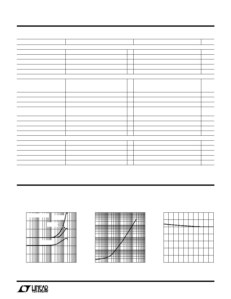
LT1120A
TEMPERATURE (
∞
C)
≠50
0
SHORT-CIRCUIT CURRENT (mA)
350
150
1120A G03
300
250
200
150
100
50
110
≠10
30
70
REGULATOR OUTPUT CURRENT (mA)
0.1
0.01
SUPPLY CURRENT (mA) 0.1
100
1
1000
1120A G02
10
1
100
10
ELECTRICAL CHARACTERISTICS
The
q
denotes specifications which apply over the operating temperature range.
Note 1: For T
A
≠40
∞
C output sink current drops to 2.5mA.
Regulator Load Regulation
Supply Current
Regulator Short-Circuit Current
TYPICAL PERFOR
M
A
N
CE CHARACTERISTICS
U
W
OUTPUT CURRENT (mA)
0.1
≠0.3
OUTPUT VOLTAGE CHANGE (%)
0.3
10
1000
1120A G01
100
1
0.2
0.1
0
≠0.1
≠0.2
T
J
= ≠55
∞
C
T
J
= 25
∞
C
T
J
= 125
∞
C
PRE-LOAD = 100
µ
A
PARAMETER
CONDITIONS
MIN
TYP
MAX
UNITS
Reference
Reference Voltage
4.5V
V
IN
36V
q
2.40
2.50
2.55
V
Line Regulation
4.5V
V
IN
36V
q
0.01
0.02
%/V
Load Regulation
≠2.0mA
I
REF
2mA, V
IN
= 12V
q
0.4
0.8
%
Output Source Current
V
IN
= 5V
q
2
mA
Output Sink Current
V
IN
= 5V
q
2
mA
Regulator
Supply Current
V
IN
= 6V, I
OUT
100
µ
A
q
30
40
µ
A
V
IN
= 36V, I
OUT
100
µ
A
q
40
50
µ
A
V
IN
= 12V, I
OUT
=
125mA
q
11
20
mA
Output Current
(V
IN
≠ V
OUT
)
1V, V
IN
6V
q
125
mA
Load Regulation
(V
IN
≠ V
OUT
)
1V, V
IN
6V
q
1
%
Line Regulation
6V
V
IN
36V
q
0.02
%/V
Dropout Voltage
I
OUT
=
100
µ
A
q
0.06
V
I
OUT
= 125mA
q
0.85
V
Feedback Sense Voltage
V
IN
= 12V
q
2.38
2.5
2.57
V
Feedback Bias Current
q
50
nA
Minimum Load Current
V
IN
= 36V
q
50
µ
A
Short Circuit Current
V
IN
= 36V
q
240
400
mA
Comparator
Offset Voltage
V
IN
= 36V
q
10
mV
Bias Current
V
IN
= 36V
q
15
60
nA
Gain
V
OUT
= 29V, R
L
= 20k
q
1000
V/V
Output Sink Current (Note 1)
V
IN
= 4.5V
q
5
10
mA
Leakage Current
V
IN
= 36V, V(Pin 7) = 36V
q
8
µ
A

4
LT1120A
REGULATOR OUTPUT CURRENT (mA)
0.1
0
FEEDBACK PIN CURRENT (nA)
40
1
1000
1120A G10
10
20
100
35
30
25
15
10
5
T
J
= ≠55
∞
C
T
J
= 25
∞
C
T
J
= 125
∞
C
REGULATOR OUTPUT CURRENT (mA)
0.1
0.01
REGULATOR INPUT-OUTPUT DIFFERENTIAL (V)
1
1
1000
1120A G04
10
0.1
100
V
OUT
= 100mV
Regulator Minimum Load Current
Regulator Ripple Rejection
Supply Current at Dropout
Reference Regulation
TYPICAL PERFOR
M
A
N
CE CHARACTERISTICS
U
W
TEMPERATURE (
∞
C)
70
1
MINIMUM LOAD CURRENT (
µ
A)
100
80
150
1120A G05
110
10
130
90
100
120
140
RIPPLE FREQUENCY (Hz)
10
30
RIPPLE REJECTION (dB)
70
1k
100k
1120A G06
10k
100
65
60
55
50
45
40
35
I
OUT
= 100mA
I
OUT
= 10mA
V
IN
= 10VDC,
1Vp-p
V
OUT
= 5V
C
OUT
= 10
µ
F
I
OUT
= 1mA
REGULATOR INPUT-OUTPUT DIFFERENTIAL (V)
0
0.01
SUPPLY CURRENT (mA)
0.1
10
0.2
0.6
1120A G08
0.3
1
0.1
0.5
I
OUT
= 100mA
I
OUT
= 10mA
I
OUT
= 1mA
0.4
REFERENCE OUTPUT CURRENT (mA)
≠1.5
≠4
REFERENCE VOLTAGE CHANGE (mV)
4
0
1.5
1120A G09
0.5
≠1.0
3
2
1
0
≠1
≠2
≠3
≠0.5
1.0
Dropout Voltage
Supply Current
REGULATOR INPUT-OUTPUT DIFFERENTIAL (V)
1
0.01
SUPPLY CURRENT (mA)
0.1
10
10
25
1120A G07
15
1
5
20
I
OUT
= 100mA
I
OUT
= 10mA
V
OUT
= 5V
I
OUT
= 1mA
Feedback Pin Current
Regulator Thermal Regulation
Turn-On Characteristic
TIME (ms)
0
OUTPUT CURRENT (mA)
0.1
180
1120A G11
80
0
≠0.1
50
0
20 40 60
100 120 140 160
OUTPUT VOLTAGE CHANGE (%)
V
IN
= 15V
V
OUT
= 5V
INPUT VOLTAGE (V)
0
5.5
1120A G12
0
OUTPUT VOLTAGE (V)
5.0
4.5
4.0
3.5
3.0
2.5
2.0
1
2
3
4
5
6
7
8
V
OUT
= 5V
NO LOAD
R
L
= 500
R
L
= 50
5
LT1120A
BLOCK DIAGRA
M
W
Pin 1 (Ground).
Pin 2 (Feedback): This is the feedback point of the
regulator. When operating, it is nominally at 2.5V.
Optimum source resistance is 200k to 500k. The feedback
pin should not be driven below ground or more positive
than 5V.
Pin 3 (Shutdown): A logic 1 shuts off main regulator.
Caution: noise or leakage into the shutdown pin can affect
output voltage.
Pin 4 (Regulator Output): Main output, requires 10
µ
F
output capacitor. Can be shorted to V
IN
or ground without
damaging device.
PI
N
FU
N
CTIO
N
S
U
U
U
Pin 5 (Input Supply): Bypass with 10
µ
F cap. Must always
be more positive than ground.
Pin 6 (Reference): 2.5V can source or sink current. May
be shorted to ground or up to 5V. Voltages in excess of 5V
can damage the device.
Pin 7 (Comparator Output): May be connected to any
voltage from ground to 36V more positive than ground
(operates above V
IN
). Short circuit protected.
Pin 8 (Comparator Input): Inverting comparator input.
≠
+
100k
5
7
6
REFERENCE
8
≠INPUT
120k
V
IN
COMPARATOR
OUT
4
V
OUT
2
FEEDBACK
3
SHUTDOWN
1
GROUND
REF
2.5V
1120A BD01
The LT1120A is especially suited for micropower system
applications. For example, the comparator section of the
LT1120A may be used as a battery checker to provide an
indication of low battery. Another type of system applica-
tion for the LT1120A would be to generate the equivalent
of split supplies off of a single power input. The regulator
section provides regulated output voltage and the
reference, which can both source and sink current is then
an artificial system ground providing a split supply for
the system.
APPLICATIO
N
S I
N
FOR
M
ATIO
N
W
U
U
U
For many applications the comparator can be frequency
compensated to operate as an amplifier. Compensation
values for various gains are given in the data sheet. The
comparator gain is purposely low to make it easier to
frequency compensate as an amplifier. The NPN output is
capable of sinking 10mA and can drive loads connected to
voltages in excess of the positive power supply. This is
useful for driving switches or linear regulators off of a
higher input voltage.