1121fb.pm6
1
LT1121/LT1121-3.3/LT1121-5
Micropower Low Dropout
Regulators with Shutdown
s
0.4V Dropout Voltage
s
150mA Output Current
s
30
µ
A Quiescent Current
s
No Protection Diodes Needed
s
Adjustable Output from 3.8V to 30V
s
3.3V and 5V Fixed Output Voltages
s
Controlled Quiescent Current in Dropout
s
Shutdown
s
16
µ
A Quiescent Current in Shutdown
s
Stable with 0.33
µ
F Output Capacitor
s
Reverse Battery Protection
s
No Reverse Current with Input Low
s
Thermal Limiting
The LT
®
1121/LT1121-3.3/LT1121-5 are micropower low
dropout regulators with shutdown. These devices are
capable of supplying 150mA of output current with a
dropout voltage of 0.4V. Designed for use in battery-
powered systems, the low quiescent current, 30
µ
A oper-
ating and 16
µ
A in shutdown, makes them an ideal choice.
The quiescent current is well-controlled; it does not rise in
dropout as it does with many other low dropout PNP
regulators.
Other features of the LT1121/LT1121-3.3/LT1121-5 in-
clude the ability to operate with very small output capaci-
tors. They are stable with only 0.33
µ
F on the output while
most older devices require between 1
µ
F and 100
µ
F for
stability. Small ceramic capacitors can be used, enhancing
manufacturability. Also the input may be connected to
ground or a reverse voltage without reverse current flow
from output to input. This makes the LT1121 series ideal
for backup power situations where the output is held high
and the input is at ground or reversed. Under these
conditions only 16
µ
A will flow from the output pin to
ground.
s
Low Current Regulator
s
Regulator for Battery-Powered Systems
s
Post Regulator for Switching Supplies
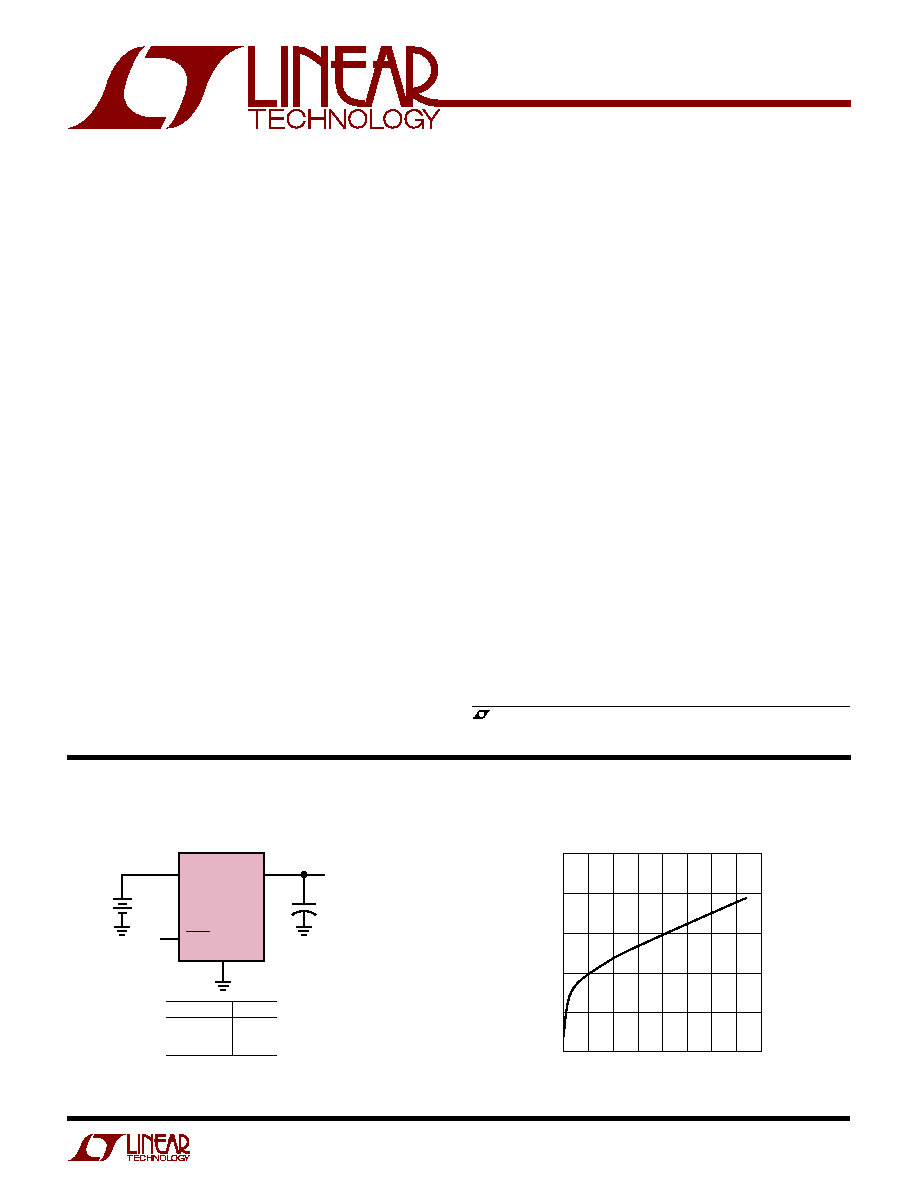
5V Battery-Powered Supply with Shutdown
OUTPUT CURRENT (mA)
0
DROPOUT VOLTAGE (V)
0.3
0.4
0.5
60
100
160
0.2
0.1
0
20
40
80
120 140
LT1121 · TA02
Dropout Voltage
IN
OUT
LT1121-3.3
GND
3.3V
OUT
150mA
1
µ
F
SOLID TANTALUM
5V
8
+
5
1
3
LT1121 · TA01
V
SHDN
(PIN 5)
<0.25
>2.8
NC
OUTPUT
OFF
ON
ON
SHDN
FEATURES
DESCRIPTIO
U
APPLICATIO S
U
TYPICAL APPLICATIO
U
, LTC and LT are registered trademarks of Linear Technology Corporation.
2
LT1121/LT1121-3.3/LT1121-5
Output Short-Circuit Duration ......................... Indefinite
Operating Junction Temperature Range (Note 3)
LT1121C-X ........................................... 0
°
C to 125
°
C
LT1121I-X ....................................... 40
°
C to 125
°
C
Storage Temperature Range ................. 65
°
C to 150
°
C
Lead Temperature (Soldering, 10 sec).................. 300
°
C
Input Voltage
LT1121 .............................................................
±
30V
LT1121HV ............................................. +36V, 30V
Output Pin Reverse Current ................................. 10mA
Adjust Pin Current ............................................... 10mA
Shutdown Pin Input Voltage (Note 2) ........ 6.5V, 0.6V
Shutdown Pin Input Current (Note 2) .................. 20mA
W
U
U
PACKAGE/ORDER I FOR ATIO
T
JMAX
= 150
°
C,
JA
150
°
C/ W
T
JMAX
= 150
°
C,
JA
50
°
C/ W
3
2
1
FRONT VIEW
TAB IS
GND
OUTPUT
GND
V
IN
ST PACKAGE
3-LEAD PLASTIC SOT-223
ORDER PART NUMBER
ORDER PART
NUMBER
LT1121CZ-3.3
LT1121IZ-3.3
LT1121CZ-5
LT1121IZ-5
Consult factory for Military grade parts.
LT1121CN8
LT1121CN8-3.3
LT1121CN8-5
LT1121IN8
LT1121IN8-3.3
LT1121IN8-5
LT1121CS8
LT1121CS8-3.3
LT1121CS8-5
LT1121HVCS8
LT1121IS8
1121
11213
11215
1121H
1121I
121I3
121I5
121IH
1121A
121A3
121A5
121AH
121AI
121AI3
121AI5
121AIH
LT1121CST-3.3
LT1121IST-3.3
LT1121CST-5
LT1121IST-5
S8 PART
MARKING
ORDER PART
NUMBER
1
2
3
4
8
7
6
5
TOP VIEW
OUT
NC/ADJ*
GND
NC
IN
NC**
NC**
SHDN
N8 PACKAGE
8-LEAD PDIP
S8 PACKAGE
8-LEAD PLASTIC SO
PIN 2 = NC FOR LT1121-3.3/LT1121-5
= ADJ FOR LT1121
PINS 6 AND 7 ARE FLOATING (NO
INTERNAL CONNECTION) ON THE
STANDARD S8 PACKAGE.
PINS 6 AND 7 CONNECTED TO GROUND
ON THE A VERSION OF THE LT1121 (S8 ONLY).
CONNECTING PINS 6 AND 7 TO THE
GROUND PLANE WILL REDUCE THERMAL
RESISTANCE. SEE THERMAL RESISTANCE
TABLES IN THE APPLICATIONS INFORMATION
SECTION.
*
**
T
JMAX
= 150
°
C,
JA
120
°
C/ W (N8, S8)
T
JMAX
= 150
°
C,
JA
70
°
C/ W (AS8)
ABSOLUTE AXI U RATI GS
W
W
W
U
(Note 1)
LT1121IS8-3.3
LT1121IS8-5
LT1121HVIS8
LT1121ACS8
LT1121ACS8-3.3
LT1121ACS8-5
LT1121AHVCS8
LT1121AIS8
LT1121AIS8-3.3
LT1121AIS8-5
LT1121AHVIS8
BOTTOM VIEW
IN
GND
OUT
Z PACKAGE
3-LEAD PLASTIC TO-92
3
LT1121/LT1121-3.3/LT1121-5
PARAMETER
CONDITIONS
MIN
TYP
MAX
UNITS
Regulated Output Voltage
LT1121-3.3
V
IN
= 3.8V, I
OUT
= 1mA, T
J
= 25
°
C
3.250
3.300
3.350
V
(Note 4)
4.3V < V
IN
< 20V, 1mA < I
OUT
< 150mA
q
3.200
3.300
3.400
V
LT1121-5
V
IN
= 5.5V, I
OUT
= 1mA, T
J
= 25
°
C
4.925
5.000
5.075
V
6V < V
IN
< 20V, 1mA < I
OUT
< 150mA
q
4.850
5.000
5.150
V
LT1121 (Note 5)
V
IN
= 4.3V, I
OUT
= 1mA, T
J
= 25
°
C
3.695
3.750
3.805
V
4.8V < V
IN
< 20V, 1mA < I
OUT
< 150mA
q
3.640
3.750
3.860
V
Line Regulation
LT1121-3.3
V
IN
= 4.8V to 20V, I
OUT
= 1mA
q
1.5
10
mV
LT1121-5
V
IN
= 5.5V to 20V, I
OUT
= 1mA
q
1.5
10
mV
LT1121 (Note 5)
V
IN
= 4.3V to 20V, I
OUT
= 1mA
q
1.5
10
mV
Load Regulation
LT1121-3.3
I
LOAD
= 1mA to 150mA, T
J
= 25
°
C
12
25
mV
I
LOAD
= 1mA to 150mA
q
20
40
mV
LT1121-5
I
LOAD
= 1mA to 150mA, T
J
= 25
°
C
17
35
mV
I
LOAD
= 1mA to 150mA
q
28
50
mV
LT1121 (Note 5)
I
LOAD
= 1mA to 150mA, T
J
= 25
°
C
12
25
mV
I
LOAD
= 1mA to 150mA
q
18
40
mV
Dropout Voltage
I
LOAD
= 1mA, T
J
= 25
°
C
0.13
0.16
V
(Note 6)
I
LOAD
= 1mA
q
0.25
V
I
LOAD
= 50mA, T
J
= 25
°
C
0.30
0.35
V
LOAD
= 50mA
q
0.50
V
I
LOAD
= 100mA, T
J
= 25
°
C
0.37
0.45
V
I
LOAD
= 100mA
q
0.60
V
I
LOAD
= 150mA, T
J
= 25
°
C
0.42
0.55
V
I
LOAD
= 150mA
q
0.70
V
Ground Pin Current
I
LOAD
= 0mA
q
30
50
µ
A
(Note 7)
I
LOAD
= 1mA
q
90
120
µ
A
I
LOAD
= 10mA
q
350
500
µ
A
I
LOAD
= 50mA
q
1.5
2.5
mA
I
LOAD
= 100mA
q
4.0
7.0
mA
I
LOAD
= 150mA
q
7.0
14.0
mA
Adjust Pin Bias Current (Notes 5, 8)
T
J
= 25
°
C
150
300
nA
Shutdown Threshold
V
OUT
= Off to On
q
1.2
2.8
V
V
OUT
= On to Off
q
0.25
0.75
V
Shutdown Pin Current (Note 9)
V
SHDN
= 0V
q
6
10
µ
A
Quiescent Current in Shutdown (Note 10)
V
IN
= 6V, V
SHDN
= 0V
q
15
22
µ
A
Ripple Rejection
V
IN
V
OUT
= 1V (Avg), V
RIPPLE
= 0.5V
P-P
,
50
58
dB
f
RIPPLE
= 120Hz, I
LOAD
= 0.1A
Current Limit
V
IN
V
OUT
= 7V, T
J
= 25
°
C
200
500
mA
Input Reverse Leakage Current
V
IN
= 20V, V
OUT
= 0V
q
1.0
mA
Reverse Output Current (Note 11)
LT1121-3.3
V
OUT
= 3.3V, V
IN
= 0V
16
25
µ
A
LT1121-5
V
OUT
= 5V, V
IN
= 0V
16
25
µ
A
LT1121 (Note 5)
V
OUT
= 3.8V, V
IN
= 0V
16
25
µ
A
The
q
denotes specifications which apply over the operating temperature
range, otherwise specifications are at T
A
= 25
°
C.
Note 2: The shutdown pin input voltage rating is required for a low
impedance source. Internal protection devices connected to the shutdown
pin will turn on and clamp the pin to approximately 7V or 0.6V. This
range allows the use of 5V logic devices to drive the pin directly. For high
Note 1: Absolute Maximum Ratings are those values beyond which the life
of a device may be impaired.
ELECTRICAL CHARACTERISTICS
4
LT1121/LT1121-3.3/LT1121-5
impedance sources or logic running on supply voltages greater than 5.5V,
the maximum current driven into the shutdown pin must be limited to less
than 20mA.
Note 3: For junction temperatures greater than 110
°
C, a minimum load of
1mA is recommended. For T
J
> 110
°
C and I
OUT
< 1mA, output voltage
may increase by 1%.
Note 4: Operating conditions are limited by maximum junction
temperature. The regulated output voltage specification will not apply for
all possible combinations of input voltage and output current. When
operating at maximum input voltage, the output current range must be
limited. When operating at maximum output current the input voltage
range must be limited.
Note 5: The LT1121 (adjustable version) is tested and specified with the
adjust pin connected to the output pin.
ELECTRICAL CHARACTERISTICS
Note 6: Dropout voltage is the minimum input/output voltage required to
maintain regulation at the specified output current. In dropout the output
voltage will be equal to: (V
IN
V
DROPOUT
).
Note 7: Ground pin current is tested with V
IN
= V
OUT
(nominal) and a
current source load. This means that the device is tested while operating
in its dropout region. This is the worst case ground pin current. The
ground pin current will decrease slightly at higher input voltages.
Note 8: Adjust pin bias current flows into the adjust pin.
Note 9: Shutdown pin current at V
SHDN
= 0V flows out of the shutdown pin.
Note 10: Quiescent current in shutdown is equal to the sum total of the
shutdown pin current (6
µ
A) and the ground pin current (9
µ
A).
Note 11: Reverse output current is tested with the input pin grounded and
the output pin forced to the rated output voltage. This current flows into
the output pin and out of the ground pin.
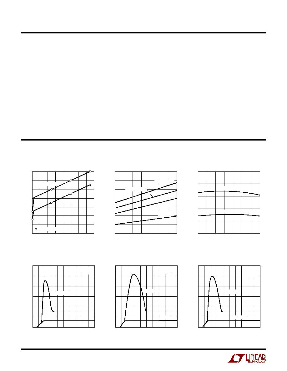
LT1121-3.3
Quiescent Current
Guaranteed Dropout Voltage
Dropout Voltage
Quiescent Current
LT1121
Quiescent Current
LT1121-5
Quiescent Current
OUTPUT CURRENT (mA)
DROPOUT VOLTAGE (V)
0.7
0.6
0.5
0.4
0.3
0.2
0.1
0
40
80
120
1121 G27
20
60
140 160
0
100
= TEST POINTS
T
J
125
°
C
T
J
25
°
C
TEMPERATURE (
°
C)
50
DROPOUT VOLTAGE (V)
0.7
0.6
0.5
0.4
0.3
0.2
0.1
0
0
50
75
1121 G14
25
25
100
125
I
LOAD
= 150mA
I
LOAD
= 50mA
I
LOAD
= 1mA
I
LLOAD
= 100mA
TEMPERATURE (
°
C)
50
QUIESCENT CURRENT (
µ
A)
10
40
30
20
10
0
0
50
75
1121 G11
25
25
100
125
V
IN
= 6V
R
LOAD
=
V
SHDN
= 0V
V
SHDN
= OPEN
INPUT VOLTAGE (V)
0
QUIESCENT CURRENT (
µ
A)
120
100
80
60
40
20
0
8
1121 G03
2
4
6
10
1
3
5
7
9
V
SHDN
= 0V
T
J
= 25
°
C
R
LOAD
=
V
OUT
= V
ADJ
V
SHDN
= OPEN
INPUT VOLTAGE (V)
0
QUIESCENT CURRENT (
µ
A)
120
100
80
60
40
20
0
8
1121 G02
2
4
6
10
1
3
5
7
9
T
J
= 25
°
C
R
LOAD
=
V
SHDN
= 0V
V
SHDN
= OPEN
INPUT VOLTAGE (V)
0
QUIESCENT CURRENT (
µ
A)
120
100
80
60
40
20
0
8
1121 G04
2
4
6
10
1
3
5
7
9
V
SHDN
= 0V
T
J
= 25
°
C
R
LOAD
=
V
SHDN
= OPEN
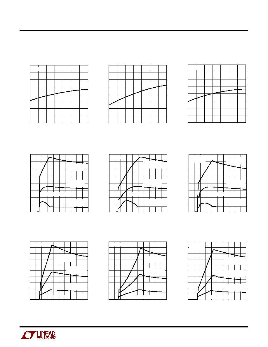
TYPICAL PERFOR A CE CHARACTERISTICS
U
W
5
LT1121/LT1121-3.3/LT1121-5
LT1121-3.3
Output Voltage
LT1121-5
Output Voltage
TEMPERATURE (
°
C)
50
OUTPUT VOLTAGE (V)
3.83
3.81
3.79
3.77
3.75
3.73
3.71
3.69
3.67
0
50
75
1121 G24
25
25
100
125
I
OUT
= 1mA
LT1121
Adjust Pin Voltage
TEMPERATURE (°C)
50
OUTPUT VOLTAGE (V)
3.38
3.36
3.34
3.32
3.30
3.28
3.26
3.24
3.22
0
50
75
1121 G22
25
25
100
125
I
OUT
= 1mA
TEMPERATURE (
°
C)
50
OUTPUT VOLTAGE (V)
5.08
5.06
5.04
5.02
5.00
4.98
4.96
4.94
4.92
0
50
75
1121 G23
25
25
100
125
I
OUT
= 1mA
TYPICAL PERFOR A CE CHARACTERISTICS
U
W
LT1121-5
Ground Pin Current
LT1121
Ground Pin Current
LT1121-3.3
Ground Pin Current
INPUT VOLTAGE (V)
0
GROUND PIN CURRENT (
µ
A)
800
700
600
500
400
300
200
100
0
8
1121 G10
2
4
6
10
1
3
5
7
9
R
LOAD
= 130
I
LOAD
= 25mA*
R
LOAD
= 330
I
LOAD
= 10mA*
R
LOAD
= 3.3k
I
LOAD
= 1mA*
T
J
= 25
°
C
*FOR V
OUT
= 3.3V
LT1121-3.3
Ground Pin Current
INPUT VOLTAGE (V)
0
GROUND PIN CURRENT (
µ
A)
800
700
600
500
400
300
200
100
0
8
1121 G06
2
4
6
10
1
3
5
7
9
T
J
= 25
°
C
R
LOAD
= 500
I
LOAD
= 10mA*
R
LOAD
= 5k
I
LOAD
= 1mA*
R
LOAD
= 200
I
LOAD
= 25mA*
*FOR V
OUT
= 5V
LT1121
Ground Pin Current
INPUT VOLTAGE (V)
0
GROUND PIN CURRENT (mA)
10
9
8
7
6
5
4
3
2
1
0
8
1121 G09
2
4
6
10
1
3
5
7
9
T
J
= 25
°
C
R
LOAD
= 22
I
LOAD
= 150mA*
R
LOAD
= 33
I
LOAD
= 100mA*
R
LOAD
= 66
I
LOAD
= 50mA*
*FOR V
OUT
= 3.3V
INPUT VOLTAGE (V)
0
GROUND PIN CURRENT (mA)
10
9
8
7
6
5
4
3
2
1
0
8
1121 G05
2
4
6
10
1
3
5
7
9
T
J
= 25
°
C
R
LOAD
= 50
I
LOAD
= 100mA*
R
LOAD
= 100
I
LOAD
= 50mA*
R
LOAD
= 33
I
LOAD
= 150mA*
*FOR V
OUT
= 5V
LT1121-5
Ground Pin Current
INPUT VOLTAGE (V)
0
GROUND PIN CURRENT (mA)
10
9
8
7
6
5
4
3
2
1
0
8
1121 G07
2
4
6
10
1
3
5
7
9
T
J
= 25
°
C
V
OUT
= V
ADJ
R
LOAD
= 25
I
LOAD
= 150mA*
R
LOAD
= 38
I
LOAD
= 100mA*
R
LOAD
= 75
I
LOAD
= 50mA*
*FOR V
OUT
= 3.75V
INPUT VOLTAGE (V)
0
GROUND PIN CURRENT (
µ
A)
800
700
600
500
400
300
200
100
0
8
1121 G08
2
4
6
10
1
3
5
7
9
T
J
= 25
°
C
V
OUT
= V
ADJ
R
LOAD
= 150
I
LOAD
= 25mA*
R
LOAD
= 380
I
LOAD
= 10mA*
R
LOAD
= 3.8k
I
LOAD
= 1mA*
*FOR V
OUT
= 3.75V