 | ÐлекÑÑоннÑй компоненÑ: LT1122DS8 | СкаÑаÑÑ:  PDF PDF  ZIP ZIP |
Äîêóìåíòàöèÿ è îïèñàíèÿ www.docs.chipfind.ru
1
LT1122
Fast Settling, JFET Input
Operational Amplifier
s
100% Tested Settling Time
340ns Typ
to 1mV at Sum Node, 10V Step
540ns Max
Tested with Fixed Feedback Capacitor
s
Slew Rate
60V/
µ
s Min
s
Gain Bandwidth Product
14MHz
s
Power Bandwidth (20Vp-p)
1.2 MHz
s
Unity Gain Stable; Phase Margin
60
°
s
Input Offset Voltage
600
µ
V Max
s
Input Bias Current
25
°
C
75pA Max
70
°
C
600pA Max
s
Input Offset Current
25
°
C
40pA Max
70
°
C
150pA Max
s
Low Distortion
D
U
ESCRIPTIO
S
FEATURE
The LT1122 JFET input operational amplifier combines
high speed and precision performance.
A unique poly-gate JFET process minimizes gate series
resistance and gate-to-drain capacitance, facilitating wide
bandwidth performance, without degrading JFET transis-
tor matching.
It slews at 80V/
µ
s and settles in 340ns. The LT1122 is
internally compensated to be unity gain stable, yet it has a
bandwidth of 14MHz at a supply current of only 7mA. Its
speed makes the LT1122 an ideal choice for fast settling
12-bit data conversion and acquisition systems.
The LT1122 offset voltage of 120
µ
V, and voltage gain of
500,000 also support the 12-bit accurate applications.
The input bias current of 10pA and offset current of 4pA
combined with its speed allow the LT1122 to be used in
such applications as high speed sample and hold amplifi-
ers, peak detectors, and integrators.
s
Fast 12-Bit D/A Output Amplifiers
s
High Speed Buffers
s
Fast Sample and Hold Amplifiers
s
High Speed Integrators
s
Voltage to Frequency Converters
s
Active Filters
s
Log Amplifiers
s
Peak Detectors
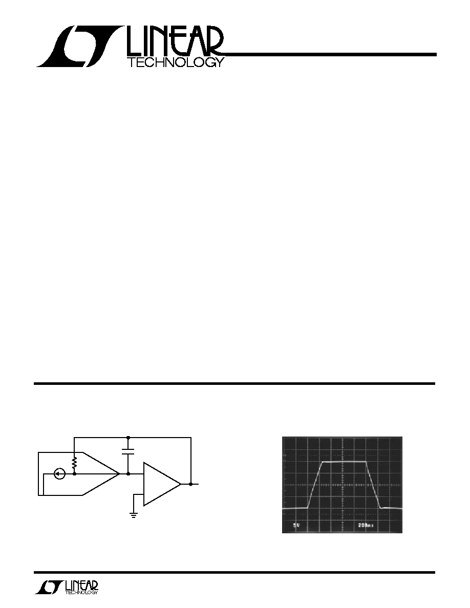
12-Bit Voltage Output D/A Converter
Large-Signal Response
5V/DIV
200ns/DIV
AV = 1
1122 TA07
U
S
A
O
PPLICATI
U
A
O
PPLICATI
TYPICAL
0mA TO 2mA
OR 4mA
+
2
3
6
Cf
V
0V TO 10V
OUT
12-BIT CURRENT OUTPUT D/A CONVERTER
C = 5pF TO 17pF
(DEPENDING ON D/A CONVERTER USED)
+
f
LT1122
LT1122·TA01
2
LT1122
Supply Voltage ....................................................
±
20V
Differential Input Voltage ......................................
±
40V
Input Voltage ........................................................
±
20V
Output Short Circuit Duration .......................... Indefinite
Lead Temperature (Soldering, 10 sec.)................. 300
°
C
Operating Temperature Range
LT1122AM/BM/CM/DM .................... 55
°
C to 125
°
C
LT1122AC/BC/CC/DC/CS/DS .............. 40
°
C to 85
°
C
Storage Temperature Range
All Devices ....................................... 65
°
C to 150
°
C
W
U
U
PACKAGE/ORDER I FOR ATIO
LT1122AMJ8 LT1122CCJ8
LT1122BMJ8 LT1122DCJ8
LT1122CMJ8 LT1122ACN8
LT1122DMJ8 LT1122BCN8
LT1122ACJ8
LT1122CCN8
LT1122BCJ8
LT1122DCN8
ORDER PART
NUMBER
ORDER PART
NUMBER
LT1122CS8
LT1122DS8
PART MARKING
1122C
1122D
A
U
G
W
A
W
U
W
A
R
BSOLUTE
XI
TI
S
8
7
6
5
4
3
2
1
V
TRIM
IN
+IN
V
V TRIM
OUT
+
V
SPEED BOOST/
OVERCOMP
TOP VIEW
N8 PACKAGE
8-LEAD PLASTIC DIP
OS
OS
LT1122
J8 PACKAGE
8-LEAD HERMETIC DIP
T
JMAX
= 150
°
C,
JA
= 130
°
C/W (N8)
T
JMAX
= 175
°
C,
JA
= 100
°
C/W (J8)
8
7
6
5
4
3
2
1
IN
V
TRIM
+IN
V TRIM
OUT
OS
V
SPEED BOOST/
OVERCOMP
TOP VIEW
S8 PACKAGE
8-LEAD PLASTIC SOIC
+
OS
V
LT1122
T
JMAX
= 150
°
C,
JA
= 190
°
C/W
Consult factory for Industrial grade parts.
ELECTRICAL C
C
HARA TERISTICS
V
S
=
±
15V, T
A
= 25
°
C, V
CM
= 0V unless otherwise noted. (Note 1)
LT1122CM/DM
LT1122AM/BM
LT1122CC/DC
LT1122AC/BC
LT1122CS/DS
SYMBOL
PARAMETER
CONDITIONS
MIN
TYP
MAX
MIN
TYP
MAX
UNITS
V
OS
Input Offset Voltage
120
600
130
900
µ
V
I
OS
Input Offset Current
4
40
5
50
pA
I
B
Input Bias Current
10
75
12
100
pA
Input Resistance
Differential
10
12
10
12
Common Mode
V
CM
= 10V to + 8V
10
12
10
12
V
CM
= + 8V to + 11V
10
11
10
11
Input Capacitance
4
4
pF
S
R
Slew Rate
A
V
= 1
60
80
50
75
V/
µ
s
Settling Time (Note 2)
+ 10V to 0V, 10V to 0V
100% Tested: A and C Grades
to 1mV at Sum Node
340
540
350
590
ns
B and D Grades to 1mV at Sum Node
350
360
ns
All Grades to 0.5mV at Sum Node
450
470
ns
GBW
Gain Bandwidth Product
14
13
MHz
Power Bandwidth
V
OUT
= 20Vp-p
1.2
1.1
MHz
A
VOL
Large Signal Voltage Gain
V
OUT
=
±
10V, R
L
= 2k
180
500
150
450
V/mV
V
OUT
=
±
10V, R
L
= 600
130
250
110
220
V/mV
CMRR
Common Mode Rejection Ratio
V
CM
=
±
10V
83
99
80
98
dB
Input Voltage Range
(Note 3)
±
10.5
±
11
±
10.5
±
11
V
PSRR
Power Supply Rejection Ratio
V
S
=
±
10V to
±
18V
86
103
82
101
dB
Input Noise Voltage
0.1Hz to 10Hz
3.0
3.3
µ
V
P-P
Input Noise Voltage Density
f
O
= 100Hz
25
27
nV/
Hz
f
O
= 10kHz
14
15
nV/
Hz
Input Noise Current Density
f
O
= 100Hz, f
O
= 10kHz
2
2
fA/
Hz
3
LT1122
ELECTRICAL C
C
HARA TERISTICS
LT1122CM/DM
LT1122AM/BM
LT1122CC/DC
LT1122AC/BC
LT1122CS/DS
SYMBOL
PARAMETER
CONDITIONS
MIN
TYP
MAX
MIN
TYP
MAX
UNITS
V
S
=
±
15V, T
A
= 25
°
C, V
CM
= 0V unless otherwise noted.
LT1122CC/DC
LT1122AC/BC
LT1122CS/DS
SYMBOL
PARAMETER
CONDITIONS
MIN
TYP
MAX
MIN
TYP
MAX
UNITS
V
OS
Input Offset Voltage
·
350
1400
400
2000
µ
V
Average Temperature Coefficient
·
5
18
6
25
µ
V/
°
C
of Input Offset Voltage
I
OS
Input Offset Current
·
12
150
15
200
pA
I
B
Input Bias Current
·
80
600
90
800
pA
A
VOL
Large Signal Voltage Gain
V
OUT
=
±
10V, R
L
2k
·
120
380
100
340
V/mV
CMRR
Common Mode Rejection Ratio
V
CM
=
±
10V
·
82
98
78
96
dB
PSRR
Power Supply Rejection Ratio
V
S
=
±
10V to
±
17V
·
84
101
80
99
dB
Input Voltage Range
·
±
10
±
10.8
±
10
±
10.8
V
V
OUT
Output Voltage Swing
R
L
= 2k
·
±
11.5
±
12.4
±
11.5
±
12.4
V
S
R
Slew Rate
A
V
= 1
·
50
70
40
65
V/
µ
s
V
S
=
±
15V, V
CM
= 0V, 0
°
C
T
A
70
°
C, unless otherwise noted. (Note 1)
LT1122AM/BM
LT1122CM/DM
SYMBOL
PARAMETER
CONDITIONS
MIN
TYP
MAX
MIN
TYP
MAX
UNITS
V
OS
Input Offset Voltage
·
650
2400
800
3400
µ
V
Average Temperature Coefficient
·
6
18
7
25
µ
V/
°
C
of Input Offset Voltage
I
OS
Input Offset Current
·
0.5
6
0.6
9
nA
I
B
Input Bias Current
·
6
25
7
35
nA
A
VOL
Large Signal Voltage Gain
V
OUT
=
±
10V, R
L
2k
·
70
230
60
200
V/mV
CMRR
Common Mode Rejection Ratio
V
CM
=
±
10V
·
80
97
76
94
dB
PSRR
Power Supply Rejection Ratio
V
S
=
±
10V to
±
17V
·
83
100
78
98
dB
Input Voltage Range
·
±
10
±
10.5
±
10
±
10.5
V
V
OUT
Output Voltage Swing
R
L
= 2k
·
±
11.3
±
12.1
±
11.3
±
12.1
V
S
R
Slew Rate
A
V
= 1
·
45
60
35
55
V/
µ
s
V
S
=
±
15V, V
CM
= 0V, 55
°
C
T
A
125
°
C, unless otherwise noted. (Note 1)
The
·
denotes the specifications which apply over the full operating
temperature range.
Note 1: The LT1122 is measured in an automated tester in less than one
second after application of power. Depending on the package used, power
dissipation, heat sinking, and air flow conditions, the fully warmed up chip
temperature can be 10
°
C to 50
°
C higher than the ambient temperature.
Note 2: Settling time is 100% tested for A and C grades using the settling
time test circuit shown. This test is not included in quality assurance
sample testing.
Note 3: Input voltage range functionality is assured by testing offset
voltage at the input voltage range limits to a maximum of 4mV (A, B
grades), to 5.7mV (C, D grades).
Note 4: Minimum supply voltage is tested by measuring offset voltage to
7mV maximum at
±
5V supplies.
Note 5: The LT1122 is not tested and not quality-assurance-sampled at
40
°
C and at 85
°
C. These specifications are guaranteed by design,
correlation and/or inference from 55
°
C, 0
°
C, 25
°
C, 70
°
C and/or 125
°
C
tests.
V
OUT
Output Voltage Swing
R
L
= 2k
±
12
±
12.5
±
12
±
12.5
V
R
L
= 600
±
11.5
±
12
±
11.5
±
12
V
I
S
Supply Current
7.5
10
7.8
11
mA
Minimum Supply voltage
(Note 4)
±
5
±
5
V
Offset Adjustment Range
R
POT
10k, Wiper to V
+
±
4
±
10
±
4
±
10
mV
4
LT1122
V
S
=
±
15V, V
CM
= 0V, 40
°
C
T
A
85
°
C, unless otherwise noted. (Note 5)
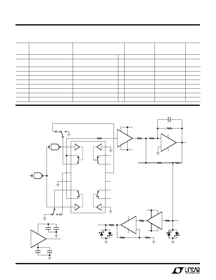
Settling Time Test Fixture
ELECTRICAL C
C
HARA TERISTICS
LT1122CC/DC
LT1122AC/BC
LT1122CS/DS
SYMBOL
PARAMETER
CONDITIONS
MIN
TYP
MAX
MIN
TYP
MAX
UNITS
V
OS
Input Offset Voltage
·
450
1900
500
2700
µ
V
Average Temperature Coefficient
·
6
20
7
28
µ
V/
°
C
of Input Offset Voltage
I
OS
Input Offset Current
·
30
600
40
900
pA
I
B
Input Bias Current
·
230
2000
260
2700
pA
A
VOL
Large Signal Voltage Gain
V
OUT
=
±
10V, R
L
2k
·
95
340
80
300
V/mV
CMRR
Common Mode Rejection Ratio
V
CM
=
±
10V
·
80
98
76
96
dB
PSRR
Power Supply Rejection Ratio
V
S
=
±
10V to
±
17V
·
83
100
78
98
dB
Input Voltage Range
·
±
10
±
10.6
±
10
±
10.6
V
V
OUT
Output Voltage Swing
R
L
= 2k
·
±
11.3
±
12.2
±
11.3
±
12.2
V
S
R
Slew Rate
A
V
= 1
·
45
65
35
60
V/
µ
s
16
15
14
13
12
11
10
9
8
7
6
5
4
3
2
1
+15V
1 F TANT
µ
0.1 F
µ
1 F TANT
µ
0.1 F
µ
TYPICAL SUPPLY
BYPASSING FOR
EACH AMP/BUFFER
10V
(REGULATED)
1
2
TTL
IN
4
5
74LS00
GROUND ALL
OTHER INPUTS
+10V
(REGULATED)
6
3
SETTLING
TIME OUTPUT
(20 TIMES SUM
NODE OUTPUT)
1k
NO CONNECTION ON PINS
10, 11, 12, 14, AND 15
1N5712
+15V
15V
1.5k
LT1223
51
+
3
2
4
7
6
8
1
7
2
5
4
51
1N5712
SUMMING
NODE
OUTPUT
15V
+15V
*THIS RESISTOR CAN BE ADJUSTED TO
NULL OUT ALL OFFSETS AT THE SETTLING
TIME OUTPUT. THE AUTOMATED TESTER
USES A SEPARATE AUTOZERO CIRCUIT.
15V
(MEASURE INPUT
PULSE HERE)
V
IN
5.1k
1%
4
15V
3
2
7
6
LT1122
+
2k
1%
+15V
2k
1%
DEVICE UNDER TEST
5pF
+15V
7
1
5
2
8
51
51
HA5002
79
5.1k*
1%
HA5002
4
LTC201A
LT1122·TA02
+
+
15V
5
LT1122
C
C
HARA TERISTICS
U
W
A
TYPICAL PERFOR
CE
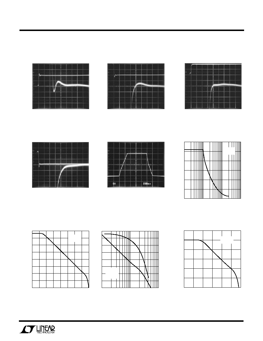
Settling Time
Settling Time
Settling Time
(Input From 10V to 0V)
(Input From +10V to 0V)
(Input From 0V to +10V)
100ns/DIV
1122 G01
100ns/DIV
1122 G02
100ns/DIV
1122 G03
1mV/DIV AT SUM NODE
1mV/DIV AT SUM NODE
1mV/DIV AT SUM NODE
200ns/DIV
A
V
= +1
1122 G05
Settling Time
Undistorted Output Swing vs
(Input From 0V to 10V)
Large Signal Response
Frequency
100ns/DIV
1122 G04
1mV/DIV AT SUM NODE
5V/DIV
FREQUENCY (Hz)
100k
0
PEAK TO PEAK OUTPUT SWING (V)
10
20
25
30
1M
10M
100M
V = ±15V
T = 25°C
15
5
S
A
LT1122·TPC01
FREQUENCY (Hz)
1
0
GAIN (dB)
20
40
60
80
100
120
10
100
1k
10k
20
40
100k 1M 10M 100M
V = ±15V
T = 25°C
S
A
LT1122·TPC02
Common Mode Rejection vs
Voltage Gain vs Frequency
Gain, Phase vs Frequency
Frequency
FREQUENCY (Hz)
1M
10
GAIN (dB)
10
20
100M
10M
0
80
100
120
140
160
180
200
V = ±15V
T = 25°C
C = 15pF
S
A
L
PHASE SHIFT (DEGREES)
LT1122·TPC03
FREQUENCY (Hz)
100
0
COMMON-MODE REJECTION RATIO (dB)
20
40
60
80
100
120
1k
10k
1M
100M
V = ±15V
T = 25°C
S
A
100k
10M
LT1122·TPC04