 | –≠–ª–µ–∫—Ç—Ä–æ–Ω–Ω—ã–π –∫–æ–º–ø–æ–Ω–µ–Ω—Ç: LT1123-5 | –°–∫–∞—á–∞—Ç—å:  PDF PDF  ZIP ZIP |

1
LT1123
Low Dropout
Regulator Driver
The LT
Æ
1123 is a 3-pin bipolar device designed to be used
in conjunction with a discrete PNP power transistor to
form an inexpensive low dropout regulator. The LT1123
consists of a trimmed bandgap reference, error amplifier,
and a driver circuit capable of sinking up to 125mA from
the base of the external PNP pass transistor. The LT1123
is designed to provide a fixed output voltage of 5V.
The drive pin of the device can pull down to 2V at 125mA
(1.4V at 10mA). This allows a resistor to be used to reduce
the base drive available to the PNP and minimize the
power dissipation in the LT1123. The drive current of the
LT1123 is folded back as the feedback pin approaches
ground to further limit the available drive current under
short-circuit conditions.
Total quiescent current for the LT1123 is only 700
µ
A. The
device is available in a low cost TO-92 package.
s
Extremely Low Dropout
s
Low Cost
s
Fixed 5V Output, Trimmed to
±
1%
s
700
µ
A Quiescent Current
s
3-Pin TO-92 Package
s
1mV Line Regulation
s
5mV Load Regulation
s
Thermal Limit
s
4A Output Current Guaranteed
5V Low Dropout Regulator
Dropout Voltage
FEATURES
DESCRIPTIO
U
, LTC and LT are registered trademarks of Linear Technology Corporation.
TYPICAL APPLICATIO
U
620
10
µ
F*
SEALED
LEAD ACID
5.4 TO 7.2V
*REQUIRED IF DEVICE IS
MORE THAN 6" FROM MAIN
FILTER CAPACITOR
OUTPUT = 5V/4A
10
µ
F
LT1123 TA01
20
REQUIRED FOR STABILITY
(LARGER VALUES INCREASE
STABILITY)
MOTOROLA
MJE1123
DRIVE
LT1123
GND
FB
+
+
OUTPUT CURRENT (A)
0
DROPOUT VOLTAGE (V)
0.3
0.4
0.5
4
LT1123 TA02
0.2
0.1
0
1
2
3
5

2
LT1123
Drive Pin Voltage (V
DRIVE
to Ground) ..................... 30V
Feedback Pin Voltage (V
FB
to Ground) .................... 30V
Operating Junction Temperature Range ... 0
∞
C to 125
∞
C
ORDER PART
NUMBER
LT1123CST
ABSOLUTE AXI U RATI GS
W
W
W
U
Storage Temperature Range ................. ≠65
∞
C to 150
∞
C
Lead Temperature (Soldering, 10 sec)................. 300
∞
C
PACKAGE/ORDER I FOR ATIO
U
U
W
(Note 1)
ORDER PART
NUMBER
LT1123CZ
ST PART MARKING
3
2
1
FRONT VIEW
TAB IS
GND
FB
GND
DRIVE
ST PACKAGE
3-LEAD PLASTIC SOT-223
BOTTOM VIEW
DRIVE
FB
GND
Z PACKAGE
3-LEAD TO-92 PLASTIC
1123
JA
AT TAB
20
∞
C/W
T
JMAX
= 125
∞
C,
JA
= 220
∞
C/W
PARAMETER
CONDITIONS
MIN
TYP
MAX
UNITS
Feedback Voltage
I
DRIVE
= 10mA, T
J
= 25
∞
C
4.90
5.00
5.10
V
5mA
I
DRIVE
100mA
3V
V
DRIVE
20V
q
4.80
5.00
5.20
V
Feedback Pin Bias Current
V
FB
= 5.00V, 2V
V
DRIVE
15V
q
300
500
µ
A
Drive Current
V
FB
= 5.20V, 2V
V
DRIVE
15V
q
0.45
1.0
mA
V
FB
= 4.80V, V
DRIVE
= 3V
q
125
170
V
FB
= 0.5V, V
DRIVE
= 3V, 0
∞
C
T
J
100
∞
C
25
100
150
Drive Pin Saturation Voltage
I
DRIVE
= 10mA, V
FB
= 4.5V
1.4
V
I
DRIVE
= 125mA, V
FB
= 4.5V
2.0
Line Regulation
5V < V
DRIVE
< 20V
q
1.0
±
20
mV
Load Regulation
I
DRIVE
= 10 to 100mA
q
≠5
≠50
mV
Temperature Coefficient of V
OUT
0.2
mV/
∞
C
Note 1: Absolute Maximum Ratings are those values beyond which the life
of the device may be impaired.
ELECTRICAL CHARACTERISTICS
The
q
denotes the specifications which apply over the full operating temperature range, otherwise specifications are at T
A
= 25
∞
C.
Consult LTC Marketing for parts specified with wider operating temperature ranges.

3
LT1123
TEMPERATURE (
∞
C)
0
100
FEEDBACK PIN BIAS CURRENT (
µ
A)
200
300
400
25
50
75
100
LT1123 G01
125
V
FB
= 5V
Feedback Pin Bias Current
vs Temperature
FEEDBACK PIN VOLTAGE (V)
0
FEEDBACK PIN BIAS CURRENT (
µ
A)
300
400
500
4
LT1123 G04
200
100
0
1
2
3
5
T
J
= 125
∞
C
T
J
= 0
∞
C
T
J
= 25
∞
C
TEMPERATURE (
∞
C)
≠50
OUTPUT VOLTAGE (V)
5.01
5.02
5.03
25
75
LT1123 G06
5.00
4.99
≠25
0
50
100
125
4.98
4.97
Output Voltage vs Temperature
TEMPERATURE (
∞
C)
0
0
MINIMUM DRIVE PIN CURRENT (
µ
A)
200
400
600
25
50
75
100
LT1123 G02
125
100
300
500
V
DRIVE
= 3V
Minimum Drive Pin Current
vs Temperature
DRIVE CURRENT (mA)
0
0
DRIVE PIN VOLTAGE (V)
1.0
2.5
40
80
100
LT1123 G05
0.5
2.0
1.5
20
60
120
140
T
J
= 125
∞
C
T
J
= 0
∞
C
T
J
= 25
∞
C
V
FB
= 4.5V
Drive Pin Saturation Voltage
vs Drive Current
C
C
HARA TERISTICS
U
W
A
TYPICAL PERFOR
CE
FEEDBACK PIN VOLTAGE (V)
0
0
DRIVE CURRENT (mA)
50
100
150
1
2
3
4
LT1123 G03
5
6
200
T
J
= 125
∞
C
T
J
= ≠50
∞
C
T
J
= 25
∞
C
V
DRIVE
= 3V
Drive Current
vs Feedback Pin Voltage
Feedback Pin Bias Current
vs Feedback Pin Voltage
U
U
U
PI FU CTIO S
Drive Pin: The drive pin serves two functions. It provides
current to the LT1123 for its internal circuitry including
start-up, bias, current limit, thermal limit and a portion of
the base drive current for the output Darlington. The sum
total of these currents (450
µ
A typical) is equal to the
minimum drive current. This current is listed in the speci-
fications as Drive Current with V
FB
= 5.2V. This is the
minimum current required by the drive pin of the LT1123.
The second function of the drive pin is to sink the base
drive current of the external PNP pass transistor. The
available drive current is specified for two conditions.
Drive current with V
FB
= 4.80V gives the range of current
available under nominal operating conditions, when the
device is regulating. Drive current with V
FB
= 0.5V gives the
range of drive current available with the feedback pin
pulled low as it would be during start-up or during a short-
circuit fault. The drive current available when the feedback
pin is pulled low is less than the drive current available
when the device is regulating (V
FB
= 5V). This can be seen
in the curve of Drive Current vs V
FB
Voltage in the Typical
Performance Characteristics curves. This can provide
some foldback in the current limit of the regulator circuit.

4
LT1123
All internal circuitry connected to the drive pin is designed
to operate at the saturation voltage of the Darlington
output driver (1.4 to 2V). This allows a resistor to be
inserted between the base of the external PNP device and
the drive pin. This resistor is used to limit the base drive to
the external PNP below the value set internally by the
LT1123, and also to help limit power dissipation in the
LT1123. The operating voltage range of this pin is from
0V to 30V. Pulling this pin below ground by more than one
V
BE
will forward bias the substrate diode of the device.
This condition can only occur if the power supply leads are
reversed and will not damage the device if the current is
limited to less than 200mA.
Feedback Pin (V
FB
): The feedback pin also serves two
functions. It provides a path for the bias current of the
reference and error amplifier and contributes a portion of
the drive current for the Darlington output driver. The sum
total of these currents is the Feedback Pin Bias Current
(300
µ
A typical). The second function of this pin is to
provide the voltage feedback to the error amplifier.
U
U
U
PI FU CTIO S
≠
+
5V
CURRENT
LIMIT
THERMAL
LIMIT
GROUND
DRIVE
FB
LT1123 SBD01
SI PLIFIED
W
BLOCK DIAGRA
W
FU CTIO AL DESCRIPTIO
U
U
U
The LT1123 is a 3-pin device designed to be used in
conjunction with a discrete PNP transistor to form an
inexpensive ultralow dropout regulator. The device incor-
porates a trimmed 5V bandgap reference, error amplifier,
a current-limited Darlington driver and an internal thermal
limit circuit. The internal circuitry connected to the drive
pin is designed to function at the saturation voltage of the
Darlington driver. This allows a resistor to be inserted in
series with the drive pin. This resistor is used to limit the
base drive to the PNP and also to limit the power dissipa-
tion in the LT1123. The value of this resistor will be defined
by the operating requirements of the regulator circuit. The
LT1123 is designed to sink a minimum of 125mA of base
current. This is sufficient base drive to form a regulator
circuit which can supply output currents up to 4A at a
dropout voltage of less than 0.75V.
5
LT1123
The LT1123 is designed to be used in conjunction with an
external PNP transistor. The overall specifications of a
regulator circuit using the LT1123 and an external PNP will
be heavily dependent on the specifications of the external
PNP. While there are a wide variety of PNP transistors
available that can be used with the LT1123, the specifica-
tions given in typical transistor data sheets are of little use
in determining overall circuit performance.
Linear Technology has solved this problem by cooperating
with Motorola to design and specify the MJE1123. This
transistor is specifically designed to work with the LT1123
as the pass element in a low dropout regulator. The
specifications of the MJE1123 reflect the capability of the
LT1123. For example, the dropout voltage of the MJE1123
is specified up to 4A collector current with base drive
currents that the LT1123 is capable of generating (20mA
to 120mA). Output currents up to 4A with dropout voltages
less than 0.75V can be guaranteed.
The following sections describe how specifications can be
determined for the basic regulator. The charts and graphs
are based on the combined characteristics of the LT1123
and the MJE1123. Formulas are included that will enable
the user to substitute other transistors that have been
characterized. A chart is supplied that lists suggested
resistor values for the most popular range of input volt-
ages and output current.
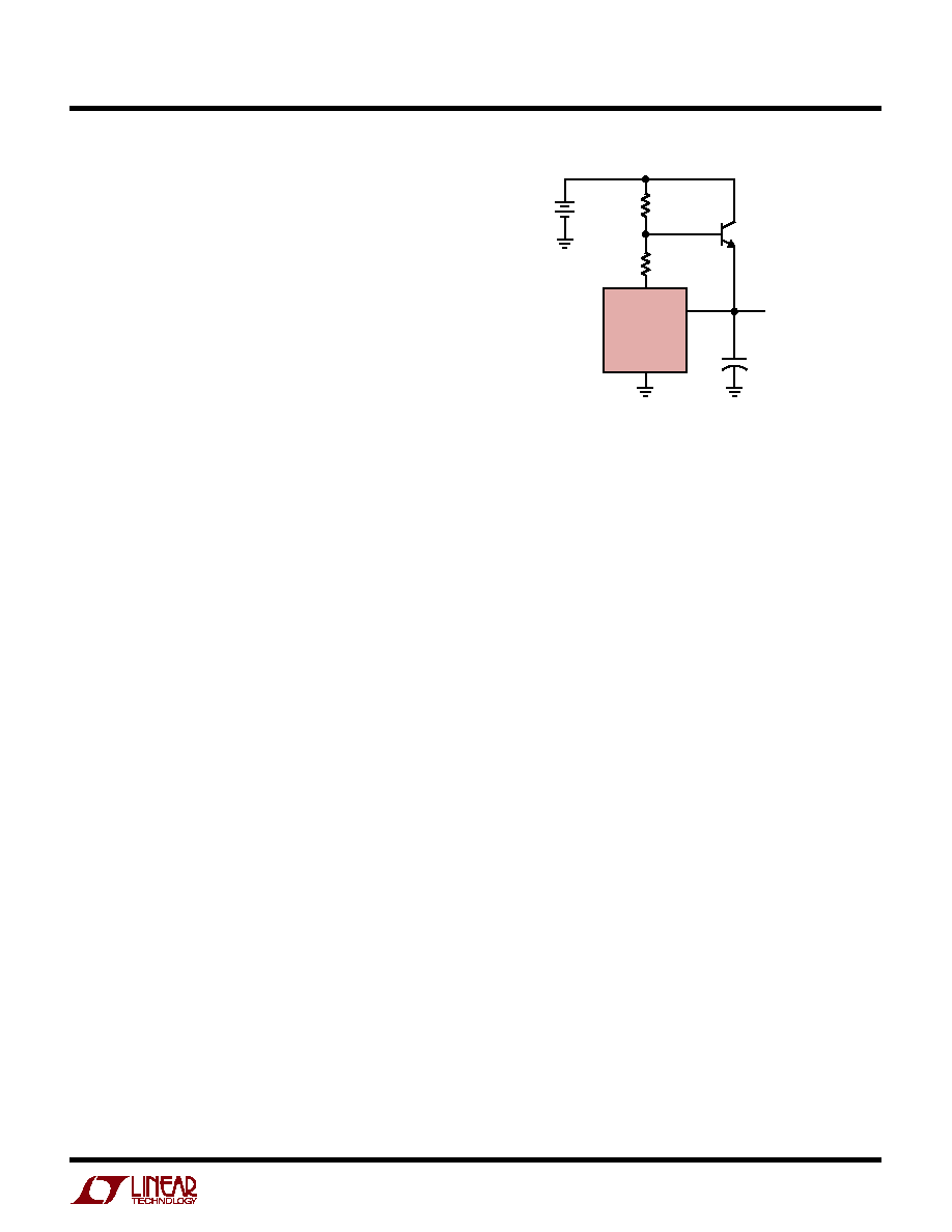
Basic Regulator Circuit
The basic regulator circuit is shown in Figure 1. The
LT1123 senses the voltage at its feedback pin and drives
the base of the PNP (MJE1123) in order to maintain the
output at 5V. The drive pin of the LT1123 can only sink
current; R
B
is required to provide pull up on the base of the
PNP. R
B
must be sized so that the voltage drop caused by
the minimum drive pin current is less than the emitter/
base voltage of the external PNP at light loads. The
recommended value for R
B
is 620
. For circuits that are
required to run at junction temperatures in excess of
100
∞
C the recommended value of R
B
is 300
.
Figure 1. Basic Regulator Circuit
R
D
is used to limit the drive current available to the PNP
and to limit the power dissipation in the LT1123. Limiting
the drive current to the PNP will limit the output current of
the regulator which will minimize the stress on the regu-
lator circuit under overload conditions. R
D
is chosen
based on the operating requirements of the circuit, prima-
rily dropout voltage and output current.
Dropout Voltage
The dropout voltage of an LT1123-based regulator circuit
is determined by the V
CE
saturation voltage of the discrete
PNP when it is driven with a base current equal to the
available drive current of the LT1123. The LT1123 can sink
up to 150mA of base current (150mA typ, 125mA min)
when output voltage is up near the regulating point (5V).
The available drive current of the LT1123 can be reduced
by adding a resistor (R
D
) in series with the drive pin (see
the section below on current limit). The MJE1123 is
specified for dropout voltage (V
CE
sat.) at several values of
output current and up to 120mA of base drive current. The
chart below lists the operating points that can be guaran-
teed by the combined data sheets of the LT1123 and
MJE1123. Figure 2 illustrates the chart in graphic form.
Although these numbers are only guaranteed by the data
sheet at 25
∞
C, Dropout Voltage vs Temperature (Figure 3)
clearly shows that the dropout voltage is nearly constant
over a wide temperature range.
R
D
R
B
620
V
IN
V
OUT
= 5V
10
µ
F ALUM
LT1123 F01
DRIVE
LT1123
GND
FB
+
MJE1123
APPLICATIO S I FOR ATIO
W
U
U
U