 | ÐлекÑÑоннÑй компоненÑ: LT1127C | СкаÑаÑÑ:  PDF PDF  ZIP ZIP |
Äîêóìåíòàöèÿ è îïèñàíèÿ www.docs.chipfind.ru
1
LT1126/LT1127
Dual/Quad
Decompensated Low Noise,
High Speed Precision Op Amps
D
U
ESCRIPTIO
S
FEATURE
s
100% Tested Low Voltage Noise
2.7nV/
Hz Typ
4.2nV/
Hz Max
s
Slew Rate
11V/
µ
s Typ
s
Gain-Bandwidth Product
65MHz Typ
s
Offset Voltage, Prime Grade
70
µ
V Max
Low Grade
100
µ
V Max
s
High Voltage Gain
5 Million Min
s
Supply Current Per Amplifier
3.1mA Max
s
Common Mode Rejection
112dB Min
s
Power Supply Rejection
116dB Min
s
Available in 8-Pin SO Package
The LT1126 dual and LT1127 quad are high performance,
decompensated op amps that offer higher slew rate and
bandwidth than the LT1124 dual and the LT1125 quad
operational amplifiers. The enhanced AC performance is
available without degrading DC specs of the LT1124/
LT1125. Both LT1126/LT1127 are stable in a gain of 10 or
more.
In the design, processing, and testing of the device,
particular attention has been paid to the optimization of the
entire distribution of several key parameters. Slew rate,
gain-bandwidth, and 1kHz noise are 100% tested for each
individual amplifier. Consequently, the specifications of
even the lowest cost grades (the LT1126C and the LT1127C)
have been enhanced.
Power consumption of the dual LT1126 is less than one
half of two OP-37s. Low power and high performance in an
8-pin SO package makes the LT1126 a first choice for
surface mounted systems and where board space is
restricted.
Protected by U.S. patents 4,775,884 and 4,837,496.
U
S
A
O
PPLICATI
s
Two and Three Op Amp Instrumentation Amplifiers
s
Low Noise Signal Processing
s
Active Filters
s
Microvolt Accuracy Threshold Detection
s
Strain Gauge Amplifiers
s
Direct Coupled Audio Gain Stages
s
Tape Head Preamplifiers
s
Microphone Preamplifiers
s
Accelerometer Amplifiers
s
Infrared Detectors
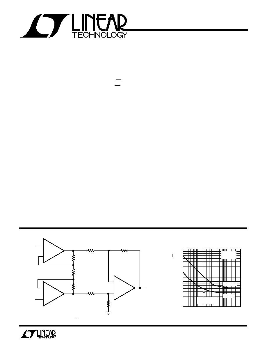
Low Noise, Wide Bandwidth Instrumentation Amplifier
GAIN = 1000, BANDWIDTH = 480kHz
INPUT REFERRED NOISE = 4.5nV/ Hz AT 1kHz, 6
µ
V
RMS
OVER BANDWIDTH
+
1/4
LT1127
LT1126 · TA01
OUTPUT
1/4
LT1127
10k
620
6.2k
200
6.2k
10k
INPUT
620
+ INPUT
1/4
LT1127
+
+
FREQUENCY (Hz)
3
RMS VOLTAGE NOISE DENSITY (nV/ Hz)
10
30
100
0.1
10
100
1000
LT1126 · TA07
1
1.0
MAXIMUM
TYPICAL
V = 15V
T = 25°C
S
A
±
1/f CORNER
2.3Hz
Voltage Noise vs Frequency
2
LT1126/LT1127
Operating Temperature Range
LT1126AM/LT1126M
LT1127AM/LT1127M ........................ 55
°
C to 125
°
C
LT1126AC/LT1126C
LT1127AC/LT1127C ............................ 40
°
C to 85
°
C
Storage Temperature Range
All Grades ......................................... 65
°
C to 150
°
C
Supply Voltage .....................................................
±
22V
Input Voltage ............................ Equal to Supply Voltage
Output Short Circuit Duration .......................... Indefinite
Differential Input Current (Note 5) ......................
±
25mA
Lead Temperature (Soldering, 10 sec.)................. 300
°
C
A
U
G
W
A
W
U
W
A
R
BSOLUTE
XI
TI
S
W
U
U
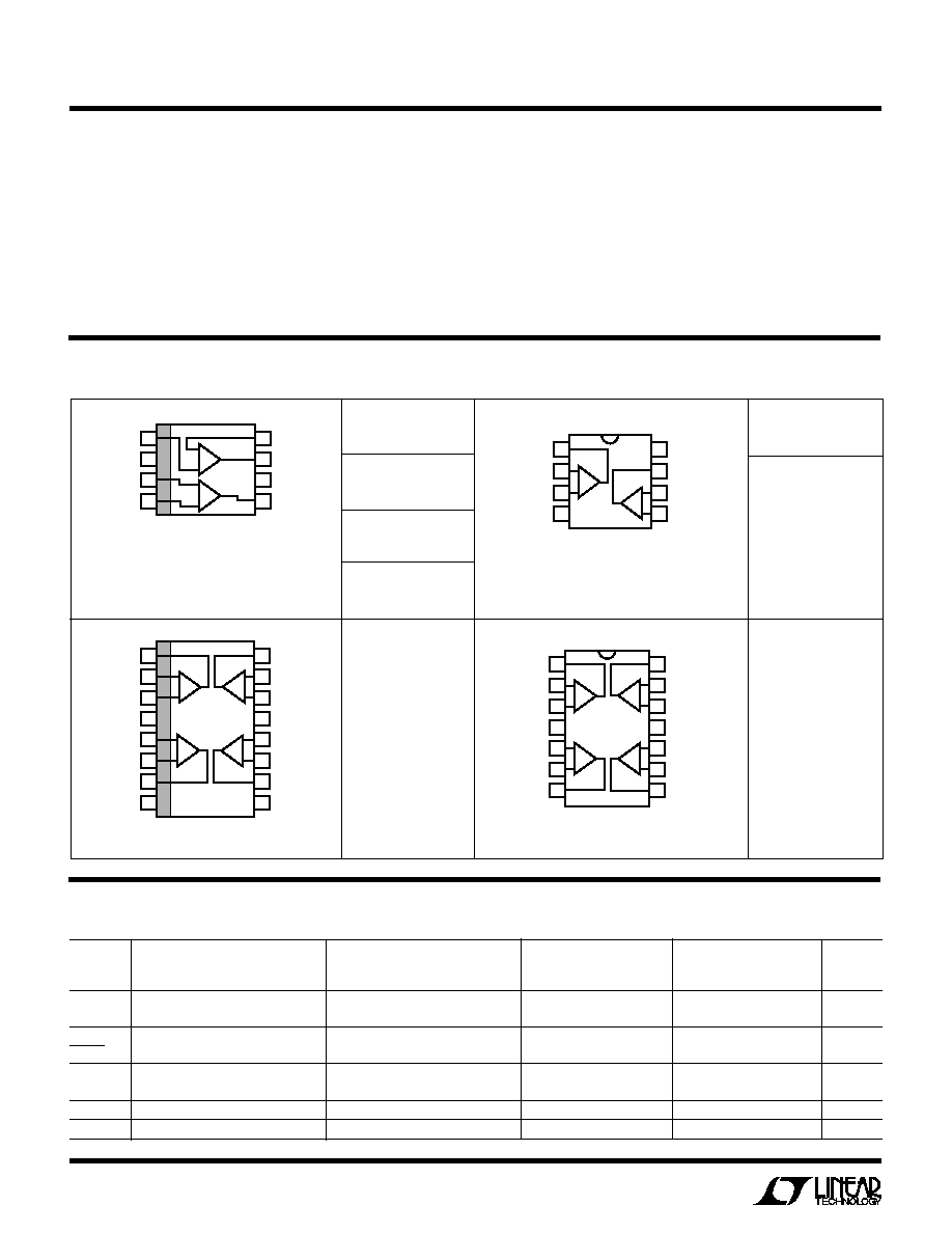
PACKAGE/ORDER I FOR ATIO
ORDER PART
NUMBER
ORDER PART
NUMBER
8
7
6
5
4
3
2
1
+
IN A
+IN A
V
TOP VIEW
N8 PACKAGE
8-LEAD PLASTIC DIP
J8 PACKAGE
8-LEAD CERAMIC DIP
OUT A
LT1126 · POI02
OUT B
V
IN B
+IN B
A
B
LT1126AM/AC
LT1126M/C
LT1127AM/AC
LT1127M/C
SYMBOL
PARAMETER
CONDITIONS (Note 1)
MIN
TYP
MAX
MIN
TYP
MAX
UNITS
V
OS
Input Offset Voltage
LT1126
20
70
25
100
µ
V
LT1127
25
90
30
140
µ
V
V
OS
Long Term Input Offset
0.3
0.3
µ
V/Mo
Time
Voltage Stability
I
OS
Input Offset Current
LT1126
5
15
6
20
nA
LT1127
6
20
7
30
nA
I
B
Input Bias Current
±
7
±
20
±
8
±
30
nA
e
n
Input Noise Voltage
0.1Hz to 10Hz (Notes 7 and 8)
70
200
70
nVp-p
V
S
=
±
15V, T
A
= 25
°
C, unless otherwise noted.
+
+IN A
V
V
8
7
6
5
4
3
2
1
+IN B
IN B
IN A
TOP VIEW
LT1126 · POI01
OUT A
A
B
OUT B
S8 PACKAGE
8-LEAD PLASTIC SOIC
NOTE: THIS PIN CONFIGURATION DIFFERS FROM THE
8-PIN DIP CONFIGURATION. INSTEAD, IT FOLLOWS
THE INDUSTRY STANDARD LT1013DS8 SO PACKAGE
PIN LOCATIONS
+
V
OUT A
IN A
+IN A
+IN B
IN B
OUT B
OUT C
V
IN D
OUT D
+IN D
+IN C
IN C
D
A
C
B
LT1126 · POI03
16
15
14
13
12
11
10
9
8
7
6
5
4
3
2
1
NC
NC
TOP VIEW
S PACKAGE
16-LEAD PLASTIC SOL
LT1126AMJ8
LT1126MJ8
LT1126CJ8
LT1126ACN8
LT1126CN8
ELECTRICAL C
C
HARA TERISTICS
N PACKAGE
14-LEAD PLASTIC DIP
J PACKAGE
14-LEAD CERAMIC DIP
LT1126 · POI04
+
V
D
14
13
12
11
10
9
8
7
6
5
4
3
2
1
OUT A
IN A
+IN A
+IN B
IN B
OUT B
OUT C
V
IN D
OUT D
TOP VIEW
A
+IN D
+IN C
IN C
C
B
LT1126CS8
S8 PART
MARKING
1126
LT1127CS
LT1127AMJ
LT1127MJ
LT1127CJ
LT1127ACN
LT1127CN
3
LT1126/LT1127
LT1126AM/AC
LT1126M/C
LT1127AM/AC
LT1127M/C
SYMBOL
PARAMETER
CONDITIONS (Note 1)
MIN
TYP
MAX
MIN
TYP
MAX
UNITS
ELECTRICAL C
C
HARA TERISTICS
V
S
=
±
15V, T
A
= 25
°
C, unless otherwise noted.
V
S
=
±
15V,
-
55
°
C
T
A
125
°
C, unless otherwise noted.
LT1126AM
LT1126M
LT1127AM
LT1127M
SYMBOL
PARAMETER
CONDITIONS (Note 1)
MIN
TYP
MAX
MIN
TYP
MAX
UNITS
V
OS
Input Offset Voltage
LT1126
q
50
170
60
250
µ
V
LT1127
q
55
190
70
290
µ
V
V
OS
Average Input Offset Voltage Drift
(Note 4)
q
0.3
1.0
0.4
1.5
µ
V/
°
C
Temp
I
OS
Input Offset Current
LT1126
q
18
45
20
60
nA
LT1127
q
18
55
20
70
nA
I
B
Input Bias Current
q
±
18
±
55
±
20
±
70
nA
V
CM
Input Voltage Range
q
±
11.3
±
12
±
11.3
±
12
V
CMRR
Common Mode Rejection Ratio
V
CM
=
±
11.3V
q
106
122
100
120
dB
PSRR
Power Supply Rejection Ratio
V
S
=
±
4V to
±
18V
q
110
122
104
120
dB
A
VOL
Large Signal Voltage Gain
R
L
10k
,
V
O
=
±
10V
q
3.0
10.0
2.0
10.0
V/
µ
V
R
L
2k
,
V
O
=
±
10V
q
1.0
3.0
0.7
2.0
V/
µ
V
V
OUT
Maximum Output Voltage Swing
R
L
2k
q
±
12.5
±
13.6
±
12.0
±
13.6
V
SR
Slew Rate
R
L
2k
(Notes 2 and 6)
q
7.2
10
7.0
10
V/
µ
s
I
S
Supply Current Per Amplifier
q
2.8
3.5
2.8
3.5
mA
ELECTRICAL C
C
HARA TERISTICS
Note 6: Slew rate is measured in A
V
= 10; input signal is
±
1V, output
measured at
±
5V.
Note 7: 0.1Hz to 10Hz noise can be inferred from the 10Hz noise voltage
density test. See the test circuit and frequency response curve for 0.1Hz to
10Hz tester in the Applications Information section of the LT1007 or
LT1028 datasheets.
Note 8: This parameter is guaranteed but not tested.
Note 9: The LT1126 and LT1127 are not tested and are not quality
assurance sampled at 40
°
C and at 85
°
C. These specifications are
guaranteed by design, correlation and/or inference from 55
°
C, 0
°
C, 25
°
C,
70
°
C and/or 125
°
C tests.
The
·
denotes the specifications which apply over the full operating
temperature range.
Note 1: Typical parameters are defined as the 60% yield of parameter
distributions of individual amplifiers; i.e., out of 100 LT1127s (or 100
LT1126s) typically 240 op amps (or 120) will be better than the indicated
specification.
Note 2: This parameter is 100% tested for each individual amplifier.
Note 3: This parameter is sample tested only.
Note 4: This parameter is not 100% tested.
Note 5: The inputs are protected by back-to-back diodes. Current limiting
resistors are not used in order to achieve low noise. If differential input
voltage exceeds
±
1.4V, the input current should be limited to 25mA.
Input Noise Voltage Density
f
O
= 10Hz (Note 3)
3.0
5.5
3.0
5.5
nV/
Hz
f
O
= 1000Hz (Note 2)
2.7
4.2
2.7
4.2
nV/
Hz
i
n
Input Noise Current Density
f
O
= 10Hz
1.3
1.3
pA/
Hz
f
O
= 1000Hz
0.3
0.3
pA/
Hz
V
CM
Input Voltage Range
±
12.0
±
12.8
±
12.0
±
12.8
V
CMRR
Common Mode Rejection Ratio
V
CM
=
±
12V
112
126
106
124
dB
PSRR
Power Supply Rejection Ratio
V
S
=
±
4V to
±
18V
116
126
110
124
dB
A
VOL
Large Signal Voltage Gain
R
L
10k
, V
O
=
±
10V
5.0
17.0
3.0
15.0
V/
µ
V
R
L
2k
, V
O
=
±
10V
2.0
4.0
1.5
3.0
V/
µ
V
V
OUT
Maximum Output Voltage Swing
R
L
2k
±
13.0
±
13.8
±
12.5
±
13.8
V
SR
Slew Rate
R
L
2k
(Notes 2 and 6)
8.0
11
8.0
11
V/
µ
s
GBW
Gain-Bandwidth Product
f
O
= 10kHz (Note 2)
45
65
45
65
MHz
Z
O
Open Loop Output Resistance
V
O
= 0, I
O
= 0
75
75
I
S
Supply Current Per Amplifier
2.6
3.1
2.6
3.1
mA
Channel Separation
f
10Hz (Note 8)
134
150
130
150
dB
V
O
=
±
10V, R
L
= 2k

4
LT1126/LT1127
V
S
=
±
15V,
-
40
°
C
T
A
85
°
C, unless otherwise noted. (Note 9)
ELECTRICAL C
C
HARA TERISTICS
V
S
=
±
15V, 0
°
C
T
A
70
°
C, unless otherwise noted.
LT1126AC
LT1126C
LT1127AC
LT1127C
SYMBOL
PARAMETER
CONDITIONS (Note 1)
MIN
TYP
MAX
MIN
TYP
MAX
UNITS
V
OS
Input Offset Voltage
LT1126
q
35
120
45
170
µ
V
LT1127
q
40
140
50
210
µ
V
V
OS
/
T
Average Input Offset Voltage Drift
(Note 4)
q
0.3
1.0
0.4
1.5
µ
V/
°
C
I
OS
Input Offset Current
LT1126
q
6
25
7
35
nA
LT1127
q
7
35
8
45
nA
I
B
Input Bias Current
q
±
8
±
35
±
9
±
45
nA
V
CM
Input Voltage Range
q
±
11.5
±
12.4
±
11.5
±
12.4
V
CMRR
Common Mode Rejection Ratio
V
CM
=
±
11.5V
q
109
125
102
122
dB
PSRR
Power Supply Rejection Ratio
V
S
=
±
4V to
±
18V
q
112
125
107
122
dB
A
VOL
Large Signal Voltage Gain
R
L
10k
,
V
O
=
±
10V
q
4.0
15.0
2.5
14.0
V/
µ
V
R
L
2k
,
V
O
=
±
10V
q
1.5
3.5
1.0
2.5
V/
µ
V
V
OUT
Maximum Output Voltage Swing
R
L
2k
q
±
12.5
±
13.7
±
12.0
±
13.7
V
SR
Slew Rate
R
L
2k
(Notes 2 and 6)
q
7.5
10.5
7.3
10.5
V/
µ
s
I
S
Supply Current Per Amplifier
q
2.7
3.3
2.7
3.3
mA
LT1126AC
LT1126C
LT1127AC
LT1127C
SYMBOL
PARAMETER
CONDITIONS (Note 1)
MIN
TYP
MAX
MIN
TYP
MAX
UNITS
V
OS
Input Offset Voltage
LT1126
q
40
140
50
200
µ
V
LT1127
q
45
160
55
240
µ
V
V
OS
/
T
Average Input Offset Voltage Drift
q
0.3
1.0
0.4
1.5
µ
V/
°
C
I
OS
Input Offset Current
LT1126
q
15
40
17
55
nA
LT1127
q
15
50
17
65
nA
I
B
Input Bias Current
q
±
15
±
50
±
17
±
65
nA
V
CM
Input Voltage Range
q
±
11.4
±
12.2
±
11.4
±
12.2
V
CMRR
Common Mode Rejection Ratio
V
CM
=
±
11.4V
q
107
124
101
121
dB
PSRR
Power Supply Rejection Ratio
V
S
=
±
4V to
±
18V
q
111
124
106
121
dB
A
VOL
Large Signal Voltage Gain
R
L
10k
,
V
O
=
±
10V
q
3.5
12.0
2.2
12.0
V/
µ
V
R
L
2k
,
V
O
=
±
10V
q
1.2
3.2
0.8
2.3
V/
µ
V
V
OUT
Maximum Output Voltage Swing
R
L
2k
q
±
12.5
±
13.6
±
12.0
±
13.6
V
SR
Slew Rate
R
L
2k
(Note 6)
q
7.3
10.2
7.1
10.2
V/
µ
s
I
S
Supply Current Per Amplifier
q
2.8
3.4
2.8
3.4
mA
ELECTRICAL C
C
HARA TERISTICS
C
C
HARA TERISTICS
U
W
A
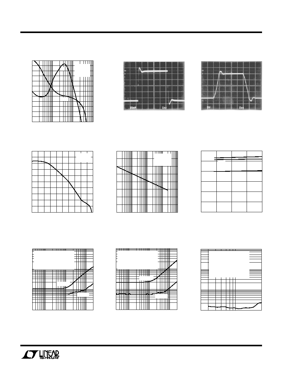
TYPICAL PERFOR
CE
The typical behavior of many LT1126/LT1127 parameters
is identical to the LT1124/LT1125. Please refer to the
LT1124/LT1125 data sheet for the following performance
characteristics:
0.1Hz to 10Hz Voltage Noise
0.01Hz to 1Hz Voltage Noise
Current Noise vs Frequency
Input Bias or Offset Current vs Temperature
Output Short Circuit Current vs Time
Input Bias Current Over the Common Mode Range
Voltage Gain vs Temperature
Input Offset Voltage Drift Distribution
Offset Voltage Drift with Temperature of Representative
Units
Output Voltage Swing vs Load Current
Common Mode Limit vs Temperature
Channel Separation vs Frequency
Warm-Up Drift
Power Supply Rejection Ratio vs Frequency
5
LT1126/LT1127
C
C
HARA TERISTICS
U
W
A
TYPICAL PERFOR
CE
*See LT1115 data sheet for definition of CCIF testing
Gain, Phase Shift vs Frequency
Small-Signal Transient Response
Large-Signal Transient Response
Common Mode Rejection Ratio vs
Voltage Gain vs Frequency
Frequency
Supply Current vs Supply Voltage
Total Harmonic Distortion
Total Harmonic Distortion
and Noise vs Frequency for
and Noise vs Frequency for
Intermodulation Distortion
Inverting Gain
Non-Inverting Gain
(CCIF Method)* vs Frequency
FREQUENCY (Hz)
TOTAL HARMONIC DISTORTION + NOISE (%)
0.010
0.1
20
1k
10k
20k
LT1126 · TPC07
100
0.001
0.0001
Z
L
= 2k/15pF
V
O
= 20Vp-p
A
V
= 10, 100
MEASUREMENT BANDWIDTH
= 10Hz TO 80kHz
A
V
= 10
A
V
= 100
FREQUENCY (Hz)
TOTAL HARMONIC DISTORTION + NOISE (%)
0.010
0.1
20
1k
10k
20k
LT1126 · TPC08
100
0.001
0.0001
Z
L
= 2k/15pF
V
O
= 20Vp-p
A
V
= +10, +100
MEASUREMENT BANDWIDTH
= 10Hz TO 80kHz
A
V
= +10
A
V
= +100
FREQUENCY (Hz)
INTERMODULATION DISTORTION (IMD) (%)
3k
10k
20k
LT1126 · TPC09
Z
L
= 2k/15pF
f (IM) = 1kHz
f
O
= 13.5kHz
V
O
= 20Vp-p
A
V
= 10
MEASUREMENT BANDWIDTH
= 10Hz TO 80kHz
LT1126
0.010
0.1
0.001
0.0001
10V
10V
A
VCL
= 10V
LT1126 · TPC03
V
S
=
±
15V
0V
50mV
50mV
0mV
FREQUENCY (MHz)
0.1
10
VOLTAGE GAIN (dB)
10
30
40
50
1.0
10
100
LT1126 · TPC01
0
20
180
140
100
80
60
160
120
PHASE SHIFT (DEGREES)
V = 15V
T = 25°C
C = 10pF
S
A
L
±
GAIN
Ø
FREQUENCY (Hz)
VOLTAGE GAIN (dB)
40
100
120
LT1126 · TPC04
1
0.01
100
10k
1M
100M
20
0
20
60
140
160
180
80
V
S
= ±15V
T
A
= 25°C
FREQUENCY (Hz)
80
COMMON MODE REJECTION RATIO (dB)
100
120
140
160
1k
100k
1M
10M
LT1126 · TPC05
10k
60
40
20
0
T
A
= 25°C
V
S
= ±15V
V
CM
= ±10V
SUPPLY VOLTAGE (V)
0
0
SUPPLY CURRENT PER AMPLIFIER (mA)
1
2
3
5
10
15
20
LT1126 · TPC06A
±
±
±
±
25°C
125°C
55°C
A
VCL
= 10V
LT1126 · TPC02
V
S
=
±
15V OR
±
5V
C
L
= 15pF