
1
LT1129/LT1129-3.3/LT1129-5
OUTPUT CURRENT (A)
0
DROPOUT VOLTAGE (V)
0.4
0.5
0.6
0.3
0.5
0.3
0.2
0.1
0.2
0.4
0.6
0.7
0.1
0
LT1129 ∑ TA02
Dropout Voltage
5V Supply with Shutdown
The LT
Æ
1129/LT1129-3.3/LT1129-5 are micropower low
dropout regulators with shutdown. The devices are ca-
pable of supplying 700mA of output current with a dropout
voltage of 0.4V at maximum output. Designed for use in
battery-powered systems the low quiescent current, 50
µ
A
operating and 16
µ
A in shutdown, make them an ideal
choice. The quiescent current does not rise in dropout as
it does with many other low dropout PNP regulators.
Other features of the LT1129 /LT1129-3.3/LT1129-5 in-
clude the ability to operate with small output capacitors.
They are stable with only 3.3
µ
F on the output while most
older devices require between 10
µ
F and 100
µ
F for stabil-
ity. Also the input may be connected to ground or a reverse
voltage without reverse current flow from output to input.
This makes the LT1129/LT1129-3.3/LT1129-5 ideal for
backup power situations where the output is held high and
the input is at ground or reversed. Under these conditions,
only 16
µ
A will flow from the output pin to ground. The
devices are available in 5-lead TO-220, 5-lead DD, 3-lead
SOT-223 and 20-lead TSSOP packages.
s
0.4V Dropout Voltage
s
700mA Output Current
s
50
µ
A Quiescent Current
s
No Protection Diodes Needed
s
Adjustable Output from 3.8V to 30V
s
3.3V and 5V Fixed Output Voltages
s
Controlled Quiescent Current in Dropout
s
Shutdown
s
16
µ
A Quiescent Current in Shutdown
s
Stable with 3.3
µ
F Output Capacitor
s
Reverse Battery Protection
s
No Reverse Output Current
s
Thermal Limiting
s
Surface Mount SOT-223 and DD Packages
s
1.1mm Thick Surface Mount TSSOP Package
s
Low Current Regulator
s
Regulator for Battery-Powered Systems
s
Post Regulator for Switching Supplies
s
5V to 3.3V Logic Regulator
IN
OUT
LT1129-5
GND
5V OUT
500mA
V
IN
> 5.5V
3.3
µ
F
SOLID TANTALUM
+
SENSE
LT1129 ∑ TA01
V
SHDN
(PIN 4)
< 0.25
> 2.8
NC
OUTPUT
OFF
ON
ON
SHDN
1
2
3
4
5
APPLICATIO S
U
FEATURES
TYPICAL APPLICATIO
U
DESCRIPTIO
U
, LTC and LT are registered trademarks of Linear Technology Corporation.
Micropower Low Dropout
Regulators with Shutdown
2
LT1129/LT1129-3.3/LT1129-5
*PIN 2 = SENSE FOR LT1129-3.3/LT1129-5
= ADJ FOR LT1129
JA
50
∞
C/ W
JA
50
∞
C/ W
*PIN 2 = SENSE FOR LT1129-3.3/LT1129-5
= ADJ FOR LT1129
JA
30
∞
C/ W
JA
60
∞
C/ W
*PIN 2 = SENSE FOR LT1129-3.3/LT1129-5
= ADJ FOR LT1129
ORDER PART
NUMBER
PART
MARKING
LT1129CST-3.3
LT1129CST-5
LT1129IST-3.3
LT1129IST-5
LT1129CT
LT1129CT-3.3
LT1129CT-5
LT1129IT
LT1129IT-3.3
LT1129IT-5
LT1129CQ
LT1129CQ-3.3
LT1129CQ-5
LT1129IQ
LT1129IQ-3.3
LT1129IQ-5
1129
11293
11295
ORDER PART
NUMBER
ORDER PART
NUMBER
LT1129CS8
LT1129CS8-3.3
LT1129CS8-5
LT1129IS8
LT1129IS8-3.3
LT1129IS8-5
Consult factory for Military grade parts.
ABSOLUTE AXI U
RATI GS
W
W
W
U
PACKAGE/ORDER I FOR ATIO
U
U
W
(Note 1)
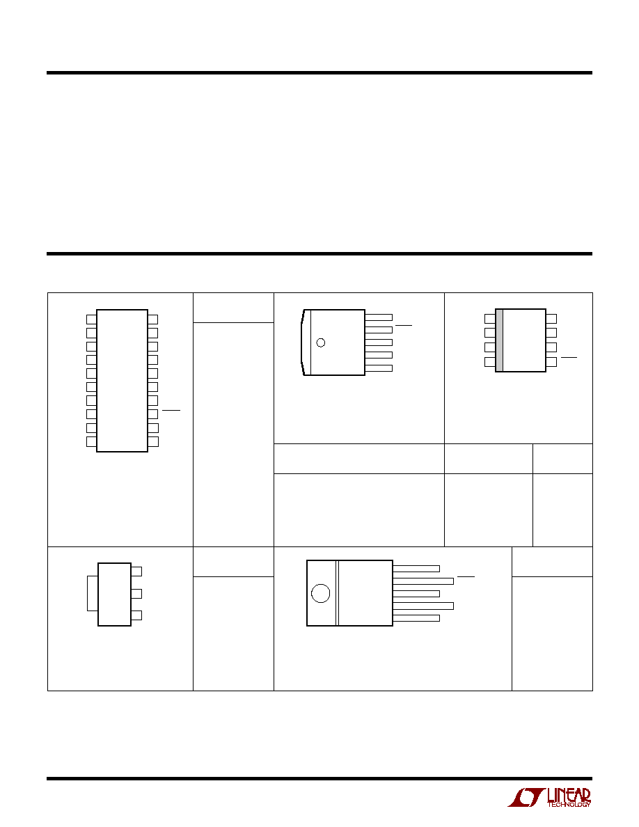
Q PACKAGE
5-LEAD PLASTIC DD
FRONT VIEW
V
IN
SHDN
GND
SENSE/ADJ*
OUTPUT
5
4
3
2
1
TAB
IS
GND
1
2
3
4
8
7
6
5
TOP VIEW
OUTPUT
GND
NC
S8 PACKAGE
8-LEAD PLASTIC SO
V
IN
GND
GND
SHDN
SENSE/
ADJ*
3
2
1
FRONT VIEW
TAB
IS
GND
ST PACKAGE
3-LEAD PLASTIC SOT-223
OUTPUT
GND
V
IN
T PACKAGE
5-LEAD PLASTIC TO-220
V
IN
SHDN
GND
SENSE/ADJ*
OUTPUT
FRONT VIEW
5
4
3
2
1
TAB
IS
GND
1
2
3
4
5
6
7
8
9
10
TOP VIEW
F PACKAGE
20-LEAD PLASTIC TSSOP
20
19
18
17
16
15
14
13
12
11
GND
GND
GND
GND
GND
GND
OUT
SENSE
GND
GND
GND
GND
GND
GND
GND
GND
IN
SHDN
GND
GND
ORDER PART
NUMBER
LT1129CF-3.3
NOTE: ALL GROUND PINS ARE
INTERNALLY CONNECTED
JA
40
∞
C/ W
Input Voltage ......................................................
±
30V*
Output Pin Reverse Current ................................. 10mA
Sense Pin Current ................................................ 10mA
Adjust Pin Current ............................................... 10mA
Shutdown Pin Input Voltage (Note 2) ........ 6.5V, ≠ 0.6V
Shutdown Pin Input Current (Note 2) .................. 20mA
Output Short-Circuit Duration ......................... Indefinite
Storage Temperature Range ................ ≠ 65
∞
C to 150
∞
C
Operating Junction Temperature Range (Note 2)
LT1129C-X ......................................... 0
∞
C to 125
∞
C
LT1129C-X Extended Temperature Range
(Note 12) ........................................ ≠40
∞
C to 125
∞
C
LT1129I-X ...................................... ≠40
∞
C to 125
∞
C
Lead Temperature (Soldering, 10 sec).................. 300
∞
C
* For applications requiring input voltage ratings greater than 30V, contact the factory.
ORDER PART
NUMBER
3
LT1129/LT1129-3.3/LT1129-5
PARAMETER
CONDITIONS
MIN
TYP
MAX
UNITS
Regulated Output Voltage
LT1129-3.3
V
IN
= 3.8V, I
OUT
= 1mA, T
J
= 25
∞
C
3.250
3.300
3.350
V
(Notes 4, 12)
4.3V < V
IN
< 20V, 1mA < I
OUT
< 700mA
q
3.200
3.300
3.400
V
LT1129-5
V
IN
= 5.5V, I
OUT
= 1mA, T
J
= 25
∞
C
4.925
5.000
5.075
V
6V < V
IN
< 20V, 1mA < I
OUT
< 700mA
q
4.850
5.000
5.150
V
LT1129 (Note 5)
V
IN
= 4.3V, I
OUT
= 1mA, T
J
= 25
∞
C
3.695
3.750
3.805
V
4.8V < V
IN
< 20V, 1mA < I
OUT
< 700mA
q
3.640
3.750
3.860
V
Line Regulation (Note 12)
LT1129-3.3
V
IN
= 4.8V to 20V, I
OUT
= 1mA
q
1.5
10
mV
LT1129-5
V
IN
= 5.5V to 20V, I
OUT
= 1mA
q
1.5
10
mV
LT1129 (Note 5)
V
IN
= 4.3V to 20V, I
OUT
= 1mA
q
1.5
10
mV
Load Regulation (Note 12)
LT1129-3.3
I
LOAD
= 1mA to 700mA, T
J
= 25
∞
C
6
20
mV
I
LOAD
= 1mA to 700mA
q
15
30
mV
LT1129-5
I
LOAD
= 1mA to 700mA, T
J
= 25
∞
C
6
20
mV
I
LOAD
= 1mA to 700mA
q
20
30
mV
LT1129 (Note 5)
I
LOAD
= 1mA to 700mA, T
J
= 25
∞
C
6
20
mV
I
LOAD
= 1mA to 700mA
q
15
30
mV
Dropout Voltage
I
LOAD
= 10mA, T
J
= 25
∞
C
0.13
0.20
V
(Note 6)
I
LOAD
= 10mA
q
0.25
V
I
LOAD
= 100mA, T
J
= 25
∞
C
0.25
0.35
V
I
LOAD
= 100mA
q
0.45
V
I
LOAD
= 500mA, T
J
= 25
∞
C
0.37
0.45
V
I
LOAD
= 500mA
q
0.60
V
I
LOAD
= 700mA, T
J
= 25
∞
C
0.45
0.55
V
I
LOAD
= 700mA
q
0.70
V
Ground Pin Current
I
LOAD
= 0mA
q
50
70
µ
A
(Note 7)
I
LOAD
= 10mA
q
310
450
µ
A
I
LOAD
= 100mA
q
2.0
3.5
mA
I
LOAD
= 300mA
q
10
20
mA
I
LOAD
= 500mA
q
25
45
mA
I
LOAD
= 700mA
q
50
90
mA
Adjust Pin Bias Current (Notes 5, 8)
T
J
= 25
∞
C
150
300
nA
Shutdown Threshold
V
OUT
= Off to On
q
1.2
2.8
V
V
OUT
= On to Off
q
0.25
0.75
V
Shutdown Pin Current (Note 9)
V
SHDN
= 0V
q
6
10
µ
A
Quiescent Current in Shutdown
V
IN
= 6V, V
SHDN
= 0V
q
15
25
µ
A
(Note 10)
Ripple Rejection
V
IN
≠ V
OUT
= 1V (Avg), V
RIPPLE
= 0.5V
P-P
,
52
64
dB
f
RIPPLE
= 120Hz, I
LOAD
= 0.7A, T
J
= 25
∞
C
Current Limit
V
IN
≠ V
OUT
= 7V, T
J
= 25
∞
C
1.2
1.6
A
Input Reverse Leakage Current
V
IN
= ≠20V, V
OUT
= 0V
q
1.0
mA
Reverse Output Current (Note 11)
LT1129-3.3
V
OUT
= 3.3V, V
IN
= 0V
16
25
µ
A
LT1129-5
V
OUT
= 5V, V
IN
= 0V
16
25
µ
A
LT1129 (Note 5)
V
OUT
= 3.8V, V
IN
= 0V
16
25
µ
A
ELECTRICAL CHARACTERISTICS
The
q
denotes the specifications which apply over the full operating
temperature range, otherwise specifications are at T
A
= 25
∞
C.

4
LT1129/LT1129-3.3/LT1129-5
Note 6: Dropout voltage is the minimum input/output voltage required to
maintain regulation at the specified output current. In dropout the output
voltage will be equal to (V
IN
≠ V
DROPOUT
). Dropout voltage is measured
between the input pin and the output pin. External voltage drops between
the output pin and the sense pin will add to the dropout voltage.
Note 7: Ground pin current is tested with V
IN
= V
OUT
(nominal) and a
current source load. This means that the device is tested while operating
in its dropout region. This is the worst case ground pin current. The
ground pin current will decrease slightly at higher input voltages.
Note 8: Adjust pin bias current flows into the adjust pin.
Note 9: Shutdown pin current at V
SHDN
= 0V flows out of the shutdown pin.
Note 10: Quiescent current in shutdown is equal to the sum total of the
shutdown pin current (6
µ
A) and the ground pin current (9
µ
A).
Note 11: Reverse output current is tested with the input pin grounded. The
output pin and the sense pin are forced to the rated output voltage. This
current flows into the sense pin and out of the ground pin. For the LT1129
(adjustable version) the sense pin is internally tied to the output pin.
Note 12: For C-grade devices Regulated Output Voltage, Line Regulation,
and Load Regulation are guaranteed over the extended temperature range
of ≠ 40
∞
C to 125
∞
C. These parameters are not tested or quality assurance
sampled at ≠40
∞
C. They are guaranteed by design, correlation and/or
inference from 25
∞
C and/or 0
∞
C tests.
Note 1: Absolute Maximum Ratings are those values beyond which the life
of a device may be impaired.
Note 2: The shutdown pin input voltage rating is required for a low
impedance source. Internal protection devices connected to the shutdown
pin will turn on and clamp the pin to approximately 7V or ≠ 0.6V. This
range allows the use of 5V logic devices to drive the pin directly. For high
impedance sources or logic running on supply voltages greater than 5.5V,
the maximum current driven into the shutdown pin must be limited to less
than 20mA.
Note 3: For junction temperatures greater than 110
∞
C, a minimum load of
1mA is recommended. For T
J
> 110
∞
C and I
OUT
< 1mA, output voltage
may increase by 1%.
Note 4: Operating conditions are limited by maximum junction
temperature. The regulated output voltage specification will not apply for
all possible combinations of input voltage and output current. When
operating at maximum input voltage, the output current range must be
limited. When operating at maximum output current the input voltage
range must be limited.
Note 5: The LT1129 is tested and specified with the adjust pin connected
to the output pin.
ELECTRICAL CHARACTERISTICS

5
LT1129/LT1129-3.3/LT1129-5
Quiescent Current
LT1129-3.3
Output Voltage
LT1129
Adjust Pin Voltage
LT1129
Quiescent Current
LT1129-5
Quiescent Current
LT1129-3.3
Quiescent Current
Guaranteed Dropout Voltage
Dropout Voltage
LT1129-5
Output Voltage
OUTPUT CURRENT (A)
DROPOUT VOLTAGE (V)
0.7
0.6
0.5
0.4
0.3
0.2
0.1
0
0.2
0.4
0.5
1129 G02
0.1
0.3
0.6
0.7
0
= TEST POINTS
T
J
125
∞
C
T
J
25
∞
C
TEMPERATURE (
∞
C)
≠50
DROPOUT VOLTAGE (V)
0.7
0.6
0.5
0.4
0.3
0.2
0.1
0
0
50
75
1129 G10
≠25
25
100
125
A
C
D
E
B
A. I
LOAD
= 700mA
B. I
LOAD
= 500mA
C. I
LOAD
= 300mA
D. I
LOAD
= 100mA
E. I
LOAD
= 10mA
TEMPERATURE (
∞
C)
≠50
QUIESCENT CURRENT (
µ
A)
70
60
50
40
30
20
10
0
0
50
75
1129 G11
≠25
25
100
125
V
SHDN
= 0V
V
SHDN
= OPEN (HI)
INPUT VOLTAGE (V)
0
QUIESCENT CURRENT (
µ
A)
250
225
200
175
150
125
100
75
50
25
0
8
1129 G13
2
4
6
10
1
3
5
7
9
V
SHDN
= 0V
I
LOAD
= 0
R
LOAD
=
V
OUT
= V
ADJ
V
SHDN
= OPEN (HI)
INPUT VOLTAGE (V)
0
QUIESCENT CURRENT (
µ
A)
250
225
200
175
150
125
100
75
50
25
0
8
1129 G14
2
4
6
10
1
3
5
7
9
V
SHDN
= 0V
I
LOAD
= 0
R
LOAD
=
V
SHDN
= OPEN (HI)
INPUT VOLTAGE (V)
0
QUIESCENT CURRENT (
µ
A)
250
225
200
175
150
125
100
75
50
25
0
8
1129 G12
2
4
6
10
1
3
5
7
9
I
LOAD
= 0
R
LOAD
=
V
SHDN
= 0V
V
SHDN
= OPEN (HI)
TEMPERATURE (
∞
C)
≠50
ADJUST PIN VOLTAGE (V)
3.400
3.375
3.350
3.325
3.300
3.275
3.250
3.225
3.200
0
50
75
1129 G06
≠25
25
100
125
I
LOAD
= 1mA
TEMPERATURE (
∞
C)
≠50
ADJUST PIN VOLTAGE (V)
3.850
3.825
3.800
3.775
3.750
3.725
3.700
3.675
3.650
0
50
75
1129 G05
≠25
25
100
125
I
LOAD
= 1mA
TEMPERATURE (
∞
C)
≠50
OUTPUT VOLTAGE (V)
5.100
5.075
5.050
5.025
5.000
4.975
4.950
4.925
4.900
0
50
75
1129 G04
≠25
25
100
125
I
LOAD
= 1mA
TYPICAL PERFOR A CE CHARACTERISTICS
U
W