
1
LT1129/LT1129-3.3/LT1129-5
Micropower Low Dropout
Regulators with Shutdown
U
A
O
PPLICATI
TYPICAL
OUTPUT CURRENT (A)
0
DROPOUT VOLTAGE (V)
0.4
0.5
0.6
0.3
0.5
0.3
0.2
0.1
0.2
0.4
0.6
0.7
0.1
0
LT1129 ∑ TA02
Dropout Voltage
5V Supply with Shutdown
D
U
ESCRIPTIO
S
FEATURE
The LT1129/LT1129-3.3/LT1129-5 are micropower low
dropout regulators with shutdown. The devices are ca-
pable of supplying 700mA of output current with a drop-
out voltage of 0.4V at maximum output. Designed for use
in battery-powered systems the low quiescent current,
50
µ
A operating and 16
µ
A in shutdown, make them
an ideal choice. The quiescent current does not rise
in dropout as it does with many other low dropout
PNP regulators.
Other features of the LT1129 /LT1129-3.3/LT1129-5 in-
clude the ability to operate with small output capacitors.
They are stable with only 3.3
µ
F on the output while most
older devices require between 10
µ
F and 100
µ
F for stabil-
ity. Also the input may be connected to ground or a reverse
voltage without reverse current flow from output to input.
This makes the LT1129/LT1129-3.3/LT1129-5 ideal for
backup power situations where the output is held high and
the input is at ground or reversed. Under these conditions,
only 16
µ
A will flow from the output pin to ground. The
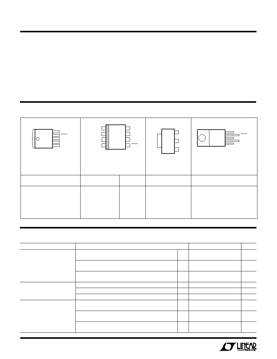
devices are available in 5-lead TO-220, 5-lead DD, and
3-lead SOT-223 packages.
s
0.4V Dropout Voltage
s
700mA Output Current
s
50
µ
A Quiescent Current
s
No Protection Diodes Needed
s
Adjustable Output from 3.8V to 30V
s
3.3V and 5V Fixed Output Voltages
s
Controlled Quiescent Current in Dropout
s
Shutdown
s
16
µ
A Quiescent Current in Shutdown
s
Stable with 3.3
µ
F Output Capacitor
s
Reverse Battery Protection
s
No Reverse Output Current
s
Thermal Limiting
s
Surface Mount
U
S
A
O
PPLICATI
s
Low Current Regulator
s
Regulator for Battery-Powered Systems
s
Post Regulator for Switching Supplies
s
5V to 3.3V Logic Regulator
IN
OUT
LT1129-5
GND
5V OUT
500mA
V
IN
> 5.5V
3.3
µ
F
SOLID TANTALUM
+
SENSE
LT1129 ∑ TA01
V
SHDN
(PIN 4)
< 0.25
> 2.8
NC
OUTPUT
OFF
ON
ON
SHDN
1
2
3
4
5
2
LT1129/LT1129-3.3/LT1129-5
A
U
G
W
A
W
U
W
A
R
BSOLUTE
XI
TI
S
PARAMETER
CONDITIONS
MIN
TYP
MAX
UNITS
Regulated Output Voltage
LT1129-3.3
V
IN
= 3.8V, I
OUT
= 1mA, T
J
= 25
∞
C
3.250
3.300
3.350
V
(Notes 3,11)
4.3V < V
IN
< 20V, 1mA < I
OUT
< 700mA
q
3.200
3.300
3.400
V
LT1129-5
V
IN
= 5.5V, I
OUT
= 1mA, T
J
= 25
∞
C
4.925
5.000
5.075
V
6V < V
IN
< 20V, 1mA < I
OUT
< 700mA
q
4.850
5.000
5.150
V
LT1129 (Note 4)
V
IN
= 4.3V, I
OUT
= 1mA, T
J
= 25
∞
C
3.695
3.750
3.805
V
4.8V < V
IN
< 20V, 1mA < I
OUT
< 700mA
q
3.640
3.750
3.860
V
Line Regulation (Note 11)
LT1129-3.3
V
IN
= 4.8V to 20V, I
OUT
= 1mA
q
1.5
10
mV
LT1129-5
V
IN
= 5.5V to 20V, I
OUT
= 1mA
q
1.5
10
mV
LT1129 (Note 4)
V
IN
= 4.3V to 20V, I
OUT
= 1mA
q
1.5
10
mV
Load Regulation (Note 11)
LT1129-3.3
I
LOAD
= 1mA to 700mA, T
J
= 25
∞
C
6
20
mV
I
LOAD
= 1mA to 700mA
q
15
30
mV
LT1129-5
I
LOAD
= 1mA to 700mA, T
J
= 25
∞
C
6
20
mV
I
LOAD
= 1mA to 700mA
q
20
30
mV
LT1129 (Note 4)
I
LOAD
= 1mA to 700mA, T
J
= 25
∞
C
6
20
mV
I
LOAD
= 1mA to 700mA
q
15
30
mV
ELECTRICAL C
C
HARA TERISTICS
Input Voltage ......................................................
±
30V*
Output Pin Reverse Current ................................. 10mA
Sense Pin Current ................................................ 10mA
Adjust Pin Current ............................................... 10mA
Shutdown Pin Input Voltage (Note 1) ........ 6.5V, ≠ 0.6V
Shutdown Pin Input Current (Note 1) .................. 20mA
Output Short-Circuit Duration ......................... Indefinite
Storage Temperature Range ................ ≠ 65
∞
C to 150
∞
C
Operating Junction Temperature Range (Note 2)
LT1129C-X ......................................... 0
∞
C to 125
∞
C
LT1129C-X Extended Temperature Range
(Note 11) ....................................... ≠40
∞
C to 125
∞
C
LT1129I-X ..................................... ≠40
∞
C to 125
∞
C
Lead Temperature (Soldering, 10 sec) .................. 300
∞
C
* For applications requiring input voltage ratings greater than 30V, contact the factory.
W
U
U
PACKAGE/ORDER I FOR ATIO
T PACKAGE
5-LEAD TO-220
V
IN
FRONT VIEW
SHDN
OUTPUT
SENSE/ADJ*
GND
TAB IS
GND
5
4
3
2
1
*PIN 2 = SENSE FOR LT1129-3.3/LT1129-5
= ADJ FOR LT1129
JA
50
∞
C/ W
JA
50
∞
C/ W
Q PACKAGE
5-LEAD DD
V
IN
SHDN
GND
SENSE/ADJ*
OUTPUT
FRONT VIEW
5
4
3
2
1
TAB
IS
GND
*PIN 2 = SENSE FOR LT1129-3.3/LT1129-5
= ADJ FOR LT1129
JA
30
∞
C/ W
1
2
3
4
8
7
6
5
TOP VIEW
OUTPUT
GND
NC
S8 PACKAGE
8-LEAD PLASTIC SO
V
IN
GND
GND
SHDN
SENSE/
ADJ*
JA
60
∞
C/ W
*PIN 2 = SENSE FOR LT1129-3.3/LT1129-5
= ADJ FOR LT1129
ORDER PART
NUMBER
PART
MARKING
LT1129CST-3.3
LT1129CST-5
LT1129IST-3.3
LT1129IST-5
LT1129CT
LT1129CT-3.3
LT1129CT-5
LT1129IT
LT1129IT-3.3
LT1129IT-5
LT1129CQ
LT1129CQ-3.3
LT1129CQ-5
LT1129IQ
LT1129IQ-3.3
LT1129IQ-5
1129
11293
11295
ORDER PART NUMBER
ORDER PART NUMBER
ORDER PART NUMBER
3
2
1
FRONT VIEW
TAB
IS
GND
OUTPUT
GND
V
IN
ST PACKAGE
3-LEAD PLASTIC SOT-223
LT1129CS8
LT1129CS8-3.3
LT1129CS8-5
LT1129IS8
LT1129IS8-3.3
LT1129IS8-5
Consult factory for Military grade parts.

3
LT1129/LT1129-3.3/LT1129-5
ELECTRICAL C
C
HARA TERISTICS
PARAMETER
CONDITIONS
MIN
TYP
MAX
UNITS
Dropout Voltage
I
LOAD
= 10mA, T
J
= 25
∞
C
0.13
0.20
V
(Note 5)
I
LOAD
= 10mA
q
0.25
V
I
LOAD
= 100mA, T
J
= 25
∞
C
0.25
0.35
V
I
LOAD
= 100mA
q
0.45
V
I
LOAD
= 500mA, T
J
= 25
∞
C
0.37
0.45
V
I
LOAD
= 500mA
q
0.60
V
I
LOAD
= 700mA, T
J
= 25
∞
C
0.45
0.55
V
I
LOAD
= 700mA
q
0.70
V
Ground Pin Current
I
LOAD
= 0mA
q
50
70
µ
A
(Note 6)
I
LOAD
= 10mA
q
310
450
µ
A
I
LOAD
= 100mA
q
2.0
3.5
mA
I
LOAD
= 300mA
q
10
20
mA
I
LOAD
= 500mA
q
25
45
mA
I
LOAD
= 700mA
q
50
90
mA
Adjust Pin Bias Current (Notes 4, 7)
T
J
= 25
∞
C
150
300
nA
Shutdown Threshold
V
OUT
= Off to On
q
1.2
2.8
V
V
OUT
= On to Off
q
0.25
0.75
V
Shutdown Pin Current (Note 8)
V
SHDN
= 0V
q
6
10
µ
A
Quiescent Current in Shutdown
V
IN
= 6V, V
SHDN
= 0V
q
15
25
µ
A
(Note 9)
Ripple Rejection
V
IN
≠ V
OUT
= 1V (Avg), V
RIPPLE
= 0.5V
P-P
,
58
64
dB
f
RIPPLE
= 120Hz, I
LOAD
= 0.7A, T
J
= 25
∞
C
Current Limit
V
IN
≠ V
OUT
= 7V, T
J
= 25
∞
C
1.2
1.6
A
Input Reverse Leakage Current
V
IN
= ≠ 20V, V
OUT
= 0V
q
1.0
mA
Reverse Output Current (Note 10)
LT1129-3.3
V
OUT
= 3.3V, V
IN
= 0V
16
25
µ
A
LT1129-5
V
OUT
= 5V, V
IN
= 0V
16
25
µ
A
LT1129 (Note 4)
V
OUT
= 3.8V, V
IN
= 0V
16
25
µ
A
voltage will be equal to (V
IN
≠ V
DROPOUT
). Dropout voltage is measured
between the input pin and the output pin. External voltage drops between
the output pin and the sense pin will add to the dropout voltage.
Note 6: Ground pin current is tested with V
IN
= V
OUT
(nominal) and a
current source load. This means that the device is tested while operating
in its dropout region. This is the worst case ground pin current. The
ground pin current will decrease slightly at higher input voltages.
Note 7: Adjust pin bias current flows into the adjust pin.
Note 8: Shutdown pin current at V
SHDN
= 0V flows out of the shutdown pin.
Note 9: Quiescent current in shutdown is equal to the sum total of the
shutdown pin current (6
µ
A) and the ground pin current (9
µ
A).
Note 10: Reverse output current is tested with the input pin grounded. The
output pin and the sense pin are forced to the rated output voltage. This
current flows into the sense pin and out of the ground pin. For the LT1129
(adjustable version) the sense pin is internally tied to the output pin.
Note 11: For C grade devices Regulated Output Voltage, Line Regulation,
and Load Regulation are guaranteed over the extended temperature range
of ≠ 40
∞
C to 125
∞
C. These parameters are not tested or quality assurance
sampled at ≠40
∞
C. They are guaranteed by design, correlation and/or
inference from 25
∞
C and/or 0
∞
C tests.
The
q
denotes specifications which apply over the operating temperature
range.
Note 1: The shutdown pin input voltage rating is required for a low
impedance source. Internal protection devices connected to the shutdown
pin will turn on and clamp the pin to approximately 7V or ≠ 0.6V. This
range allows the use of 5V logic devices to drive the pin directly. For high
impedance sources or logic running on supply voltages greater than 5.5V,
the maximum current driven into the shutdown pin must be limited to less
than 20mA.
Note 2: For junction temperatures greater than 110
∞
C, a minimum load of
1mA is recommended. For T
J
> 110
∞
C and I
OUT
< 1mA, output voltage
may increase by 1%.
Note 3: Operating conditions are limited by maximum junction
temperature. The regulated output voltage specification will not apply for
all possible combinations of input voltage and output current. When
operating at maximum input voltage, the output current range must be
limited. When operating at maximum output current the input voltage
range must be limited.
Note 4: The LT1129 is tested and specified with the adjust pin connected
to the output pin.
Note 5: Dropout voltage is the minimum input/output voltage required to
maintain regulation at the specified output current. In dropout the output

4
LT1129/LT1129-3.3/LT1129-5
C
C
HARA TERISTICS
U
W
A
TYPICAL PERFOR
CE
Quiescent Current
LT1129-3.3
Output Voltage
LT1129
Adjust Pin Voltage
LT1129
Quiescent Current
LT1129-5
Quiescent Current
LT1129-3.3
Quiescent Current
Guaranteed Dropout Voltage
Dropout Voltage
LT1129-5
Output Voltage
OUTPUT CURRENT (A)
DROPOUT VOLTAGE (V)
0.7
0.6
0.5
0.4
0.3
0.2
0.1
0
0.2
0.4
0.5
1129 G02
0.1
0.3
0.6
0.7
0
= TEST POINTS
T
J
125∞C
T
J
25∞C
TEMPERATURE (∞C)
≠50
DROPOUT VOLTAGE (V)
0.7
0.6
0.5
0.4
0.3
0.2
0.1
0
0
50
75
1129 G10
≠25
25
100
125
A
C
D
E
B
A. I
LOAD
= 700mA
B. I
LOAD
= 500mA
C. I
LOAD
= 300mA
D. I
LOAD
= 100mA
E. I
LOAD
= 10mA
TEMPERATURE (∞C)
≠50
QUIESCENT CURRENT (
µ
A)
70
60
50
40
30
20
10
0
0
50
75
1129 G11
≠25
25
100
125
V
SHDN
= 0V
V
SHDN
= OPEN (HI)
INPUT VOLTAGE (V)
0
QUIESCENT CURRENT (
µ
A)
250
225
200
175
150
125
100
75
50
25
0
8
1129 G13
2
4
6
10
1
3
5
7
9
V
SHDN
= 0V
I
LOAD
= 0
R
LOAD
=
V
OUT
= V
ADJ
V
SHDN
= OPEN (HI)
INPUT VOLTAGE (V)
0
QUIESCENT CURRENT (
µ
A)
250
225
200
175
150
125
100
75
50
25
0
8
1129 G14
2
4
6
10
1
3
5
7
9
V
SHDN
= 0V
I
LOAD
= 0
R
LOAD
=
V
SHDN
= OPEN (HI)
INPUT VOLTAGE (V)
0
QUIESCENT CURRENT (
µ
A)
250
225
200
175
150
125
100
75
50
25
0
8
1129 G12
2
4
6
10
1
3
5
7
9
I
LOAD
= 0
R
LOAD
=
V
SHDN
= 0V
V
SHDN
= OPEN (HI)
TEMPERATURE (∞C)
≠50
ADJUST PIN VOLTAGE (V)
3.400
3.375
3.350
3.325
3.300
3.275
3.250
3.225
3.200
0
50
75
1129 G06
≠25
25
100
125
I
LOAD
= 1mA
TEMPERATURE (∞C)
≠50
ADJUST PIN VOLTAGE (V)
3.850
3.825
3.800
3.775
3.750
3.725
3.700
3.675
3.650
0
50
75
1129 G05
≠25
25
100
125
I
LOAD
= 1mA
TEMPERATURE (∞C)
≠50
OUTPUT VOLTAGE (V)
5.100
5.075
5.050
5.025
5.000
4.975
4.950
4.925
4.900
0
50
75
1129 G04
≠25
25
100
125
I
LOAD
= 1mA

5
LT1129/LT1129-3.3/LT1129-5
C
C
HARA TERISTICS
U
W
A
TYPICAL PERFOR
CE
INPUT VOLTAGE (V)
0
GROUND PIN CURRENT (mA)
2.0
1.8
1.6
1.4
1.2
1.0
0.8
0.6
0.4
0.2
0
8
1129 G20
2
4
6
10
1
3
5
7
9
R
LOAD
= 75
I
LOAD
= 50mA*
R
LOAD
= 375
I
LOAD
= 10mA*
R
LOAD
= 38
I
LOAD
= 100mA*
*For V
OUT
= 3.75V
T
J
= 25∞C
V
OUT
=
V
ADJ
INPUT VOLTAGE (V)
0
GROUND PIN CURRENT (mA)
2.0
1.8
1.6
1.4
1.2
1.0
0.8
0.6
0.4
0.2
0
8
1129 G19
2
4
6
10
1
3
5
7
9
R
LOAD
= 100
I
LOAD
= 50mA*
R
LOAD
= 500
I
LOAD
= 10mA*
R
LOAD
= 50
I
LOAD
= 100mA*
*For V
OUT
= 5V
T
J
= 25∞C
V
OUT
= V
SENSE
LT1129
Ground Pin Current
LT1129-5
Ground Pin Current
LT1129-3.3
Ground Pin Current
INPUT VOLTAGE (V)
0
GROUND PIN CURRENT (mA)
2.0
1.8
1.6
1.4
1.2
1.0
0.8
0.6
0.4
0.2
0
8
1129 G18
2
4
6
10
1
3
5
7
9
R
LOAD
= 66
I
LOAD
= 50mA*
R
LOAD
= 330
I
LOAD
= 10mA*
R
LOAD
= 33
I
LOAD
= 100mA*
T
J
= 25∞C
V
OUT
=
V
SENSE
*For V
OUT
= 3.3V
LT1129-3.3
Ground Pin Current
INPUT VOLTAGE (V)
0
GROUND PIN CURRENT (mA)
60
50
40
30
20
10
0
8
1129 G22
2
4
6
10
1
3
5
7
9
R
LOAD
= 10
I
LOAD
= 500mA*
R
LOAD
= 16.6
I
LOAD
= 300mA*
R
LOAD
= 7.1
I
LOAD
= 700mA*
*For V
OUT
= 5V
T
J
= 25∞C
V
OUT
= V
SENSE
LT1129-5
Ground Pin Current
INPUT VOLTAGE (V)
0
GROUND PIN CURRENT (mA)
60
50
40
30
20
10
0
8
1129 G23
2
4
6
10
1
3
5
7
9
R
LOAD
= 7.5
I
LOAD
= 500mA*
R
LOAD
= 12.6
I
LOAD
= 300mA*
R
LOAD
= 5.3
I
LOAD
= 700mA*
*For V
OUT
= 3.75V
T
J
= 25∞C
V
OUT
= V
ADJ
LT1129
Ground Pin Current
Ground Pin Current
OUTPUT CURRENT (A)
0
GROUND PIN CURRENT (mA)
70
60
50
40
30
20
10
0
0.2
0.4
0.5
1129 G15
0.1
0.3
0.6
0.7
T
J
= 25∞C
T
J
= 125∞C
T
J
= ≠50∞C
V
IN
= 3.3V (LT1129-3.3)
V
IN
= 5V (LT1129-5)
V
IN
= 3.75V (LT1129)
DEVICE IS OPERATING
IN DROPOUT
TEMPERATURE (∞C)
≠50
SHUTDOWN THRESHOLD (V)
2.0
1.8
1.6
1.4
1.2
1.0
0.8
0.6
0.4
0.2
0
0
50
75
1129 G27
≠25
25
100
125
I
LOAD
= 1mA
Shutdown Pin Threshold
(On-to-Off)
Shutdown Pin Threshold
(Off-to-On)
TEMPERATURE (∞C)
≠50
SHUTDOWN THRESHOLD (V)
2.0
1.8
1.6
1.4
1.2
1.0
0.8
0.6
0.4
0.2
0
0
50
75
1129 G26
≠25
25
100
125
I
LOAD
= 1mA
I
LOAD
= 700mA
INPUT VOLTAGE (V)
0
GROUND PIN CURRENT (mA)
60
50
40
30
20
10
0
8
1129 G21
2
4
6
10
1
3
5
7
9
R
LOAD
= 6.6
I
LOAD
= 500mA*
R
LOAD
= 11
I
LOAD
= 300mA*
R
LOAD
= 4.7
I
LOAD
= 700mA*
*For V
OUT
= 3.3V
T
J
= 25∞C
V
OUT
= V
SENSE

6
LT1129/LT1129-3.3/LT1129-5
C
C
HARA TERISTICS
U
W
A
TYPICAL PERFOR
CE
FREQUENCY (Hz)
RIPPLE REJECTION (dB)
100
90
80
70
60
50
40
30
20
10
0
10
1k
10k
1M
1129 G01
100
100k
I
OUT
= 500mA
V
IN
= 6V + 50mV
RMS
RIPPLE
C
OUT
= 47
µ
F
SOLID
TANTALUM
C
OUT
= 3.3
µ
F
SOLID
TANTALUM
Shutdown Pin Current
SHUTDOWN PIN VOLTAGE (V)
0
0
SHUTDOWN PIN INPUT CURRENT (mA)
5
15
20
25
2
4
5
9
1129 G24
10
1
3
6
7
8
Shutdown Pin Input Current
Adjust Pin Bias Current
Current Limit
TEMPERATURE (∞C)
≠50
SHORT-CIRCUIT CURRENT (A)
1.4
1.2
1.0
0.8
0.6
0.4
0.2
0
0
50
75
1129 G08
≠25
25
100
125
V
IN
= 7V
V
OUT
= 0V
Current Limit
INPUT VOLTAGE (V)
0
SHORT-CIRCUIT CURRENT (A)
1.4
1.2
1.0
0.8
0.6
0.4
0.2
0
2
4
5
1129 G07
1
3
6
7
V
OUT
= 0V
Reverse Output Current
Reverse Output Current
Ripple Rejection
Ripple Rejection
TEMPERATURE (∞C)
≠50
RIPPLE REJECTION (dB)
70
68
66
64
62
60
58
56
0
50
75
1129 G03
≠25
25
100
125
(V
IN
≠ V
OUT
)
AVG
= 1V
V
RIPPLE
= 0.5V
P-P
I
L
= 0.7A
TEMPERATURE (∞C)
≠50
OUTPUT CURRENT (
µ
A)
30
25
20
15
10
5
0
0
50
75
1129 G29
≠25
25
100
125
V
IN
= 0V
V
OUT
= V
SENSE
= 5V (LT1129-5)
V
OUT
= V
SENSE
= 3.3V (LT1129-3.3)
V
OUT
= V
ADJ
= 3.75V (LT1129)
TEMPERATURE (∞C)
≠50
ADJUST PIN BIAS CURRENT (nA)
400
350
300
250
200
150
100
50
0
0
50
75
1129 G28
≠25
25
100
125
V
ADJ
= V
OUT
= 3.75V
OUTPUT VOLTAGE (V)
0
OUTPUT CURRENT (
µ
A)
100
90
80
70
60
50
40
30
20
10
0
8
1129 G30
2
4
6
10
1
3
5
7
9
T
J
= 25∞C, V
IN
= 0V
V
OUT
= V
SENSE
(LT1129-3.3/LT1129-5)
V
OUT
= V
ADJ
(LT1129)
CURRENT FLOWS
INTO DEVICE
LT1129-3.3
LT1129
LT1129-5
TEMPERATURE (∞C)
≠50
SHUTDOWN PIN CURRENT (
µ
A)
10
9
8
7
6
5
4
3
2
1
0
0
50
75
1129 G25
≠25
25
100
125
V
SHDN
= 0V

7
LT1129/LT1129-3.3/LT1129-5
C
C
HARA TERISTICS
U
W
A
TYPICAL PERFOR
CE
LT1129-5
Transient Response
Load Regulation
PI FU CTIO S
U
U
U
Input Pin: Power is supplied to the device through the
input pin. The input pin should be bypassed to ground if
the device is more than 6 inches away from the main input
filter capacitor. In general, the output impedance of a
battery rises with frequency so it is advisable to include a
bypass capacitor in battery-powered circuits. A bypass
capacitor in the range of 1
µ
F to 10
µ
F is sufficient. The
LT1129 is designed to withstand reverse voltages on the
input pin with respect to both ground and the output pin.
In the case of a reversed input, which can happen if a
battery is plugged in backwards, the LT1129 will act as if
there is a diode in series with its input. There will be no
reverse current flow into the LT1129 and no reverse
voltage will appear at the load. The device will protect both
itself and the load.
Output Pin: The output pin supplies power to the load. An
output capacitor is required to prevent oscillations. See
the Applications Information section for recommended
value of output capacitance and information on reverse
output characteristics.
Shutdown Pin (SHDN): This pin is used to put the device
into shutdown. In shutdown the output of the device is
turned off. This pin is active low. The device will be shut
down if the shutdown pin is actively pulled low. The
shutdown pin current with the pin pulled to ground will be
6
µ
A. The shutdown pin is internally clamped to 7V and ≠
0.6V (one V
BE
). This allows the shutdown pin to be driven
directly by 5V logic or by open collector logic with a pull-
up resistor. The pull-up resistor is only required to supply
the leakage current of the open collector gate, normally
several microamperes. Pull-up current must be limited to
a maximum of 20mA. A curve of shutdown pin input
current as a function of voltage appears in the Typical
Performance Characteristics. If the shutdown pin is not
used it can be left open circuit. The device will be active,
output on, if the shutdown pin is not connected.
Sense Pin: For fixed voltage versions of the LT1129
(LT1129-3.3, LT1129-5) the sense pin is the input to the
error amplifier. Optimum regulation will be obtained at the
point where the sense pin is connected to the output pin.
For most applications the sense pin is connected directly
to the output pin at the regulator. In critical applications
small voltage drops caused by the resistance (R
P
) of PC
traces between the regulator and the load, which would
normally degrade regulation, may be eliminated by con-
necting the sense pin to the output pin at the load as shown
in Figure 1 (Kelvin Sense Connection). Note that the
voltage drop across the external PC traces will add to the
dropout voltage of the regulator. The sense pin bias
TIME (ms)
0
OUTPUT VOLTAGE
DEVIATION (V)
0.2
0.1
0
≠0.1
≠0.2
1.6
1129 G32
0.2
0.8
1.2
2.0
0.7
0.5
0.3
0.1
LOAD CURRENT
(A)
0.4 0.6
1.0
1.4
1.8
V
IN
= 6V
C
IN
= 3.3
µ
F
C
OUT
= 47
µ
F
LT1129-5
Transient Response
TIME (
µ
s)
0
OUTPUT VOLTAGE
DEVIATION (V)
0.10
0.05
0
≠0.05
≠0.10
400
1129 G31
50
200
300
500
0.6
0.5
LOAD CURRENT
(A)
100 150
250
350
450
V
IN
= 6V
C
IN
= 3.3
µ
F
C
OUT
= 3.3
µ
F
TEMPERATURE (∞C)
≠50
LOAD REGULATION (mV)
0
≠5
≠10
≠15
≠20
≠25
≠30
0
50
75
1129 G09
≠25
25
100
125
LT1129*
LT1129-3.3
LT1129-5
V
IN
= V
OUT
(NOMINAL) + 1V
I
LOAD
= 1mA to 700mA
*V
ADJ
= V
OUT

8
LT1129/LT1129-3.3/LT1129-5
PI FU CTIO S
U
U
U
U
S
A
O
PPLICATI
W
U
U
I FOR ATIO
The LT1129 is a micropower low dropout regulator with
shutdown, capable of supplying 700mA of output current
at a dropout voltage of 0.4V. The device operates with very
low quiescent current (50
µ
A). In shutdown the quiescent
current drops to only 16
µ
A. In addition to the low quies-
cent current the LT1129 incorporates several protection
features which make it ideal for use in battery-powered
systems. The device is protected against reverse input
voltages. In battery backup applications where the output
can be held up by a backup battery when the input is pulled
to ground, the LT1129 acts like it has a diode in series with
its output and prevents reverse current flow.
Adjustable Operation
The adjustable version of the LT1129 has an output
voltage range of 3.75V to 30V. The output voltage is set by
the ratio of two external resistors as shown in Figure 2. The
device servos the output voltage to maintain the voltage at
the adjust pin at 3.75V. The current in R1 is then equal to
3.75V/R1. The current in R2 is equal to the sum of the
current in R1 and the adjust pin bias current. The adjust pin
bias current, 150nA at 25
∞
C, flows through R2 into the
adjust pin. The output voltage can be calculated according
to the formula in Figure 2. The value of R1 should be less
than 400k to minimize errors in the output voltage caused
by the adjust pin bias current. Note that in shutdown the
output is turned off and the divider current will be zero.
Curves of Adjust Pin Voltage vs Temperature and Adjust
Pin Bias Current vs Temperature appear in the Typical
Performance Characteristics. The reference voltage at the
adjust pin has a positive temperature coefficient of ap-
proximately 15ppm/
∞
C. The adjust pin bias current has a
negative temperature coefficient. These effects are small
and will tend to cancel each other.
The adjustable device is specified with the adjust pin tied
to the output pin. This sets the output voltage to 3.75V.
Specifications for output voltages greater than 3.75V will
be proportional to the ratio of the desired output voltage to
3.75V (V
OUT
/3.75V). For example: load regulation for an
output current change of 1mA to 700mA is ≠ 6mV typical
at V
OUT
= 3.75V. At V
OUT
= 12V, load regulation would be:
12
3 75
6
19
V
V
mV
mV
.
≠
≠
◊
(
)
=
(
)
IN
LT1129
GND
SHDN
LT1129 ∑ F02
+
ADJ
OUT
R2
R1
V
OUT
= 3.75V 1 + + I
ADJ
∑ R2
V
ADJ
= 3.75V
I
ADJ
= 150nA at 25∞C
OUTPUT RANGE = 3.75V to 30V
R2
R1
( )
(
)
V
OUT
Figure 2. Adjustable Operation
Figure 1. Kelvin Sense Connection
current is 15
µ
A at the nominal regulated output voltage.
This pin is internally clamped to ≠ 0.6V (one V
BE
).
Adjust Pin: For the LT1129 (adjustable version) the adjust
pin is the input to the error amplifier. This pin is internally
clamped to 6V and ≠ 0.6V (one V
BE
). This pin has a bias
current of 150nA which flows into the pin. See Bias Current
curve in the Typical Performance Characteristics. The
adjust pin reference voltage is equal to 3.75V referenced
to ground.
IN
LT1129
GND
SHDN
LT1129 ∑ F01
SENSE
OUT
R
P
+
1
µ
F
LOAD
+
10
µ
F
R
P

9
LT1129/LT1129-3.3/LT1129-5
U
S
A
O
PPLICATI
W
U
U
I FOR ATIO
Thermal Considerations
The power handling capability of the device will be limited
by the maximum rated junction temperature (125
∞
C). The
power dissipated by the device will be made up of two
components:
1. Output current multiplied by the input/output voltage
differential: I
OUT
◊
(V
IN
≠ V
OUT
), and
2. Ground pin current multiplied by the input voltage:
I
GND
◊
V
IN
.
The ground pin current can be found by examining the
Ground Pin Current curves in the Typical Performance
Characteristics. Power dissipation will be equal to the sum
of the two components listed above.
The LT1129 series regulators have internal thermal limit-
ing designed to protect the device during overload condi-
tions. For continuous normal load conditions the maxi-
mum junction temperature rating of 125
∞
C must not be
exceeded. It is important to give careful consideration to
all sources of thermal resistance from junction to ambient.
Additional heat sources mounted nearby must also be
considered.
For surface mount devices heat sinking is accomplished
by using the heat spreading capabilities of the PC board
and its copper traces. Experiments have shown that the
heat spreading copper layer does not need to be electri-
cally connected to the tab of the device. The PC material
can be very effective at transmitting heat between the pad
area, attached to the tab of the device, and a ground or
power plane layer either inside or on the opposite side of
the board. Although the actual thermal resistance of the PC
material is high, the length/area ratio of the thermal
resistor between layers is small. Copper board stiffeners
and plated through holes can also be used to spread the
heat generated by power devices.
The following tables list thermal resistances for each
package. For the TO-220 package, thermal resistance is
given for junction-to-case only since this package is
usually mounted to a heat sink. Measured values of
thermal resistance for several different board sizes and
copper areas are listed for each package. All measure-
ments were taken in still air on 3/32" FR-4 board with 1-oz
copper. This data can be used as a rough guideline in
estimating thermal resistance. The thermal resistance for
each application will be affected by thermal interactions
with other components as well as board size and shape.
Some experimentation will be necessary to determine the
actual value.
Table 1. Q Package, 5-Lead DD
COPPER AREA
TOPSIDE*
BACKSIDE
BOARD AREA
2500 sq. mm 2500 sq. mm
2500 sq. mm
25
∞
C/W
1000 sq. mm 2500 sq. mm
2500 sq. mm
27
∞
C/W
125 sq. mm
2500 sq. mm
2500 sq. mm
35
∞
C/W
* Tab of device attached to topside copper
THERMAL RESISTANCE
(JUNCTION-TO-AMBIENT)
Table 2. ST Package, 3-Lead SOT-223
COPPER AREA
TOPSIDE*
BACKSIDE
BOARD AREA
2500 sq. mm 2500 sq. mm
2500 sq. mm
45
∞
C/W
1000 sq. mm 2500 sq. mm
2500 sq. mm
45
∞
C/W
225 sq. mm
2500 sq. mm
2500 sq. mm
53
∞
C/W
100 sq. mm
2500 sq. mm
2500 sq. mm
59
∞
C/W
* Tab of device attached to topside copper
THERMAL RESISTANCE
(JUNCTION-TO-AMBIENT)
Table 3. S8 Package, 8-Lead Plastic SOIC
COPPER AREA
TOPSIDE*
BACKSIDE
BOARD AREA
2500 sq. mm 2500 sq. mm
2500 sq. mm
55
∞
C/W
1000 sq. mm 2500 sq. mm
2500 sq. mm
55
∞
C/W
225 sq. mm
2500 sq. mm
2500 sq. mm
63
∞
C/W
100 sq. mm
2500 sq. mm
2500 sq. mm
69
∞
C/W
* Device attached to topside copper
THERMAL RESISTANCE
(JUNCTION-TO-AMBIENT)
T Package, 5-Lead TO-220
Thermal Resistance (Junction-to-Case) = 5
∞
C/W
Calculating Junction Temperature
Example: Given an output voltage of 3.3V, an input voltage
range of 4.5V to 5.5V, an output current range of 0mA to
500mA, and a maximum ambient temperature of 50
∞
C,
what will the maximum junction temperature be?
The power dissipated by the device will be equal to:
I
OUT MAX
◊
(V
IN MAX
≠ V
OUT
) + (I
GND
◊
V
IN MAX
)
where, I
OUT MAX
= 500mA
V
IN MAX
= 5.5V
I
GND
at (I
OUT
= 500mA, V
IN
= 5.5V) = 25mA

10
LT1129/LT1129-3.3/LT1129-5
U
S
A
O
PPLICATI
W
U
U
I FOR ATIO
so,
P = 500mA
◊
(5.5V ≠ 3.3V) + (25mA
◊
5.5V)
= 1.24W
If we use a DD package, then the thermal resistance will be
in the range of 25
∞
C/W to 35
∞
C/W depending on copper
area. So the junction temperature rise above ambient will
be approximately equal to:
1.24W
◊
30
∞
C/W = 37.2
∞
C
The maximum junction temperature will then be equal to
the maximum junction temperature rise above ambient
plus the maximum ambient temperature or:
T
JMAX
= 50
∞
C + 37.2
∞
C = 87.2
∞
C
Output Capacitance and Transient Performance
The LT1129 is designed to be stable with a wide range of
output capacitors. The minimum recommended value is
3.3
µ
F with an ESR of 2
or less. The LT1129 is a
micropower device and output transient response will be
a function of output capacitance. See the Transient Re-
sponse curves in the Typical Performance Characteristics.
Larger values of output capacitance will decrease the peak
deviations and provide improved output transient re-
sponse. Bypass capacitors, used to decouple individual
components powered by the LT1129, will increase the
effective value of the output capacitor.
Protection Features
The LT1129 incorporates several protection features which
make it ideal for use in battery-powered circuits. In addi-
tion to the normal protection features associated with
monolithic regulators, such as current limiting and ther-
mal limiting, the device is protected against reverse input
voltages, and reverse voltages from output to input. For
fixed voltage devices the output and sense pins are tied
together at the output.
Current limit protection and thermal overload protection
are intended to protect the device against current overload
conditions at the output of the device. For normal opera-
tion, the junction temperature should not exceed 125
∞
C.
The input of the device will withstand reverse voltages of
30V. Current flow into the device will be limited to less than
1mA (typically less than 100
µ
A) and no negative voltage
will appear at the output. The device will protect both itself
and the load. This provides protection against batteries
that can be plugged in backwards.
For fixed voltage versions of the device, the sense pin is
internally clamped to one diode drop below ground. For
the adjustable version of the device, the output pin is
internally clamped at one diode drop below ground. If the
output pin of an adjustable device, or the sense pin of a
fixed voltage device, is pulled below ground, with the input
open or grounded, current must be limited to less than
5mA.
In circuits where a backup battery is required, several
different input/output conditions can occur. The output
voltage may be held up while the input is either pulled to
ground, pulled to some intermediate voltage, or is left
open circuit. Current flow back into the output will vary
depending on the conditions. Many battery-powered cir-
cuits incorporate some form of power management. The
following information will help optimize battery life. Table
3 summarizes the following information.
Output current will be minimized if the input pin of the
LT1129 is pulled to ground when the output is held high.
Figure 3 shows reverse output current as a function of
output voltage with the input pin pulled to ground. This
current flows through the device to ground. This curve will
hold as long as the input pin is pulled below about 0.8V or
if the impedance from the input pin to ground is less than
50k
. The state of the shutdown pin will have no effect on
output current when the input pin is pulled to ground.
In some applications it may be necessary to leave the input
to the LT1129 unconnected when the output is held high.
This can happen when the LT1129 is powered from a
rectified AC source. If the AC source is removed, then the
input of the LT1129 is effectively left floating. In this
configuration the reverse output current is slightly higher.
It is roughly equal to the normal quiescent current. Note
that in this configuration the state of the shutdown pin has
a significant effect on the output current. Pulling the
shutdown pin to ground will minimize the output current
in this configuration. Figure 4 shows output current as a
function of output voltage with the input pin floating (open
circuit or connected to an input bypass capacitor) and the

11
LT1129/LT1129-3.3/LT1129-5
U
S
A
O
PPLICATI
W
U
U
I FOR ATIO
Information furnished by Linear Technology Corporation is believed to be accurate and reliable.
However, no responsibility is assumed for its use. Linear Technology Corporation makes no represen-
tation that the interconnection of its circuits as described herein will not infringe on existing patent rights.
OUTPUT VOLTAGE (V)
0
OUTPUT PIN CURRENT (
µ
A)
100
90
80
70
60
50
40
30
20
10
0
8
1129 F03
2
4
6
10
1
3
5
7
9
T
J
= 25∞C
V
IN
= 0V
V
SENSE
= V
OUT
CURRENT FLOWS
INTO DEVICE
LT1129-3.3
LT1129
LT1129-5
Figure 5. Reverse Output Current
Figure 3. Reverse Output Current
INPUT VOLTAGE (V)
0
350
300
250
200
150
100
50
0
3
1129 F06
1
2
5
OUTPUT CURRENT (
µ
A)
4
LT1129-3.3
V
OUT
= 3.3V
V
SENSE
= V
OUT
LT1129-5
V
OUT
= 5V
Figure 6. Reverse Output Current
OUTPUT VOLTAGE (V)
0
40
35
30
25
20
15
10
5
0
3
1129 F05
1
2
5
OUTPUT CURRENT (
µ
A)
4
LT1129-3.3
LT1129-5
V
IN
= OPEN
V
SHDN
= 0V
V
SENSE
= V
OUT
OUTPUT VOLTAGE (V)
0
350
300
250
200
150
100
50
0
3
1129 F04
1
2
5
OUTPUT CURRENT (
µ
A)
4
V
IN
= OPEN
V
SHDN
= OPEN
V
SENSE
= V
OUT
LT1129-3.3
LT1129-5
Figure 4. Reverse Output Current
shutdown pin floating (open circuit). Figure 5 shows
output current as a function of output voltage with the
input floating and the shutdown pin pulled to ground.
When the input of the LT1129 is forced to a voltage below
its nominal output voltage and its output is held high, the
output current will follow the curve shown in Figure 6 . This
can happen if the input of the LT1129 is connected to a
discharged (low voltage) battery and the output is held up
by either a backup battery or by a second regulator circuit.
Users with applications requiring lower reverse currents
should contact the factory about the availability of a
modified version of the LT1129.
Table 4. Fault Conditions
INPUT PIN
SHDN PIN
OUTPUT/SENSE PINS
0.8V
Open (Hi)
Forced to V
OUT
(Nominal)
Reverse Output Current
15
µ
A (See Figure 3)
0.8V
Grounded
Forced to V
OUT
(Nominal)
Reverse Output Current
15
µ
A (See Figure 3)
Open
Open (Hi)
> 1V
Reverse Output Current
200
µ
A Peak (See Figure 4)
Open
Grounded
> 1V
Reverse Output Current
35
µ
A at V
OUT
= V
OUT
(Nominal)
(See Figure 5)
0.8V
V
IN
V
OUT
Open (Hi)
Forced to V
OUT
(Nominal)
Reverse Output Current
300
µ
A Peak (See Figure 6)
0.8V
V
IN
V
OUT
Grounded
Forced to V
OUT
(Nominal)
Reverse Output Current
300
µ
A (See Figure 6)

12
LT1129/LT1129-3.3/LT1129-5
Linear Technology Corporation
1630 McCarthy Blvd., Milpitas, CA 95035-7487
(408) 432-1900
q
FAX
: (408) 434-0507
q
TELEX
: 499-3977
©
LINEAR TECHNOLOGY CORPORATION 1994
LT/GP 0394 5K REV A ∑ PRINTED IN USA
PACKAGE DESCRIPTIO
U
Dimensions in inches (millimeters) unless otherwise noted.
S8 Package, 8-Lead Plastic SOIC
T Package, 5-Lead TO-220
Q Package, 5-Lead DD
0.028 ≠ 0.035
(0.711 ≠ 0.889)
0.057 ≠ 0.077
(1.448 ≠ 1.956)
0.139 ≠ 0.153
(3.531 ≠ 3.886)
DIA
0.079 ≠ 0.135
(2.007 ≠ 3.429)
0.380 ≠ 0.420
(9.652 ≠ 10.668)
0.970 ≠ 1.050
(24.64 ≠ 26.67)
0.560 ≠ 0.650
(14.224 ≠ 16.510)
0.866 ≠ 0.913
(21.996 ≠ 23.190)
0.700 ≠ 0.728
(17.780 ≠ 18.491)
0.035 ≠ 0.055
(0.889 ≠ 1.397)
0.169 ≠ 0.185
(4.293 ≠ 4.699)
0.079 ≠ 0.115
(2.007 ≠ 2.921)
0.620 ± 0.020
(15.75 ± 0.508)
0.460 ≠ 0.500
(11.68 ≠ 12.70)
0.210 ≠ 0.240
(5.334 ≠ 6.096)
0.055 ≠ 0.090
(1.397 ≠ 2.286)
0.015 ≠ 0.025
(0.381 ≠ 0.635)
0.181
(4.60)
NOM
0.025 ≠ 0.033
(0.64 ≠ 0.84)
0.071
(1.80)
MAX
10∞
MAX
0.012
(0.31)
MIN
0.0008 ≠ 0.0040
(0.0203 ≠ 0.1016)
10∞ ≠ 16∞
0.010 ≠ 0.014
(0.25 ≠ 0.36)
10∞ ≠ 16∞
0.116 ≠ 0.124
(2.95 ≠ 3.15)
0.248 ≠ 0.264
(6.30 ≠ 6.71)
0.130 ≠ 0.146
(3.30 ≠ 3.71)
0.264 ≠ 0.287
(6.71 ≠ 7.29)
0.090
(2.29)
NOM
0.033 ≠ 0.041
(0.84 ≠ 1.04)
1
2
3
4
0.150 ≠ 0.157
(3.810 ≠ 3.988)
8
7
6
5
0.189 ≠ 0.197
(4.801 ≠ 5.004)
0.228 ≠ 0.244
(5.791 ≠ 6.197)
0.010 ≠ 0.020
(0.254 ≠ 0.508)
0.016 ≠ 0.050
0.406 ≠ 1.270
◊
45
∞
0∞≠ 8∞ TYP
0.008 ≠ 0.010
(0.203 ≠ 0.254)
0.053 ≠ 0.069
(1.346 ≠ 1.752)
0.014 ≠ 0.019
(0.355 ≠ 0.483)
0.004 ≠ 0.010
(0.101 ≠ 0.254)
0.050
(1.270)
BSC
0.022 ± 0.005
(0.559 ± 0.127)
0.105 ± 0.008
(2.667 ± 0.203)
0.004
+0.008
≠0.004
(
)
0.102
+0.203
≠0.102
0.050 ± 0.012
(1.270 ± 0.305)
0.059
(1.499)
TYP
0.050 ± 0.008
(1.270 ± 0.203)
0.175 ± 0.008
(4.445 ± 0.203)
0.060
(1.524)
0.401 ± 0.015
(10.185 ± 0.381)
15∞ TYP
0.032 ± 0.008
(0.813 ± 0.203)
0.331
+0.012
≠0.020
(
)
8.407
+0.305
≠0.508
0.143
+0.012
≠0.020
(
)
3.632
+0.305
≠0.508
0.067 ± 0.010
(1.702 ± 0.254)
ST Package, 3-Lead SOT-223