 | ÐлекÑÑоннÑй компоненÑ: LT1161CS | СкаÑаÑÑ:  PDF PDF  ZIP ZIP |
Äîêóìåíòàöèÿ è îïèñàíèÿ www.docs.chipfind.ru
1
LT1161
Quad Protected High-Side
MOSFET Driver
s
Fully Enhances N-Channel MOSFET Switches
s
8V to 48V Power Supply Range
s
Protected from 15V to 60V Supply Transients
s
Individual Short-Circuit Protection
s
Individual Automatic Restart Timers
s
Programmable Current Limit, Delay Time, and
Auto-Restart Period
s
Voltage-Limited Gate Drive
s
Defaults to OFF State with Open Input
s
Flowthrough Input to Output Pinout
s
Available in 20-Lead DIP or SOL Package
The LT1161 is a quad high-side gate driver allowing the
use of low cost N-channel power MOSFETs for high-side
switching applications. It has four independent switch
channels, each containing a completely self-contained
charge pump to fully enhance an N-channel MOSFET
switch with no external components.
Also included in each switch channel is a drain sense
comparator that is used to sense switch current. When a
preset current level is exceeded, the switch is turned off.
The switch remains off for a period of time set by an
external timing capacitor and then automatically attempts
to restart. If the fault is still present, this cycle repeats until
the fault is removed, thus protecting the MOSFET.
The LT1161 has been specifically designed for harsh
operating environments such as industrial, avionics, and
automotive applications where poor supply regulation
and/or transients may be present. The device will not
sustain damage from supply voltages of 15V to 60V.
FEATURES
DESCRIPTIO
N
U
s
Industrial Control
s
Avionics Systems
s
Automotive Switches
s
Stepper Motor and DC Motor Control
s
Electronic Circuit Breaker
APPLICATIO
N
S
U
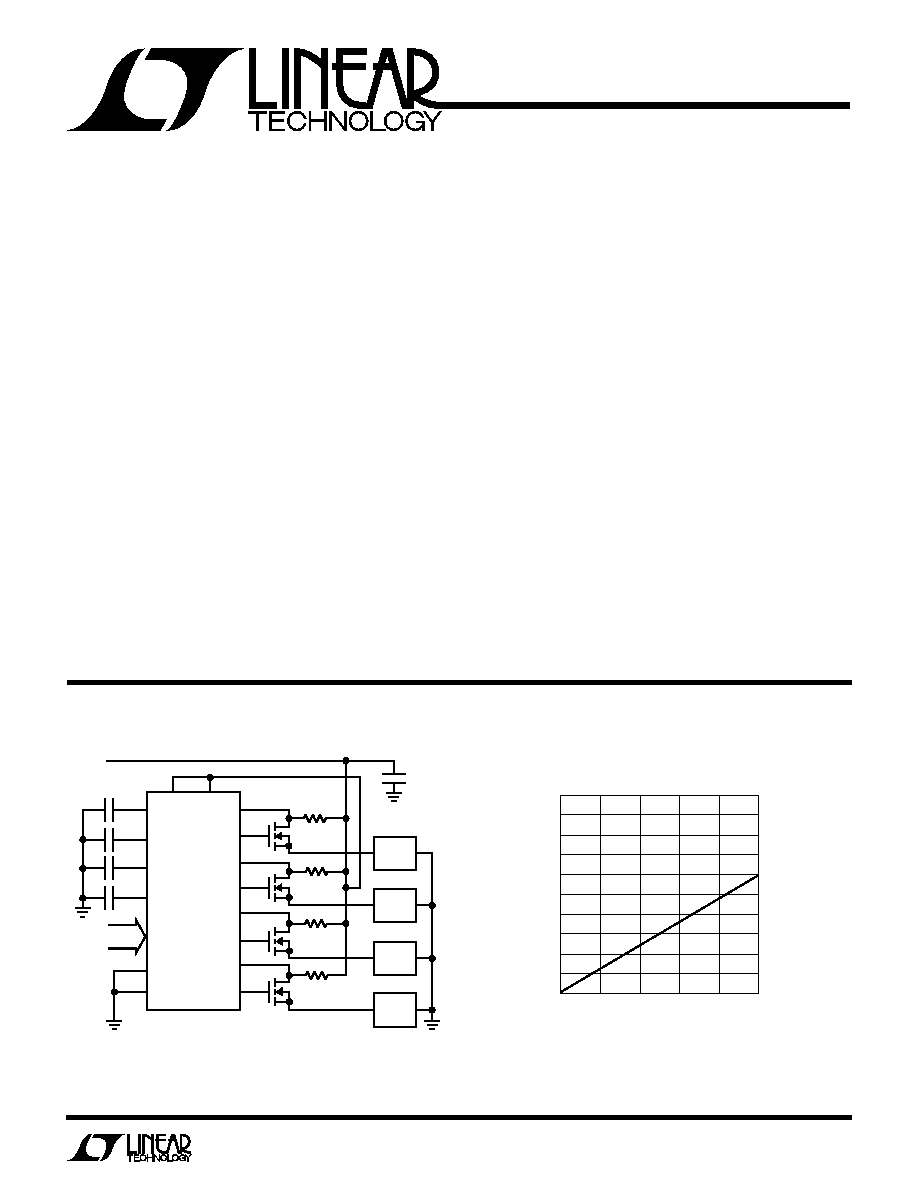
TYPICAL APPLICATIO
N
U
+
C
T
0.1
µ
F
0.1
µ
F
0.1
µ
F
0.1
µ
F
0.01
IRFZ34
24V
INPUTS
1161 F01
IRFZ34
IRFZ34
IRFZ34
R
S
0.01
0.01
0.01
LOAD
#1
50
µ
F
50V
LOAD
#2
LOAD
#3
LOAD
#4
DS1
G1
DS2
G2
DS3
G3
DS4
G4
V
+
V
+
T1
T2
T3
T4
GND
GND
IN1
IN2
IN3
IN4
LT1161
Switch Drop vs Load Current
LOAD CURRENT (A)
0
TOTAL DROP (V)
0.50
0.45
0.40
0.35
0.30
0.25
0.20
0.15
0.10
0.05
0
4
1161 TA01
1
2
3
5
Figure 1. Protected Quad High-Side Switch
2
LT1161
Supply Voltages (Pins 11, 20) ................... 15V to 60V
Input Voltages (Pins 3, 5, 7, 9) ...... (GND 0.3V) to 15V
Gate Voltages (Pins 12, 14, 16, 18) ........................ 75V
Sense Voltages (Pins 13, 15, 17, 19).................. V
+
±
5V
Current (Any Pin) .................................................. 50mA
Operating Temperature Range
LT1161C ............................................... 0
°
C to 70
°
C
LT1161I ............................................ 40
°
C to 85
°
C
Junction Temperature Range (Note 1)
LT1161C .............................................. 0
°
C to 125
°
C
LT1161I ......................................... 40
°
C to 150
°
C
Storage Temperature Range ................. 65
°
C to 150
°
C
Lead Temperature (Soldering, 10 sec).................. 300
°
C
ABSOLUTE
M
AXI
M
U
M
RATINGS
W
W
W
U
PACKAGE/ORDER I
N
FOR
M
ATIO
N
W
U
U
JA
= 70
°
C/ W (N)
JA
= 110
°
C/ W (S)
ORDER PART
NUMBER
LT1161CN
LT1161CS
LT1161IN
LT1161IS
1
2
3
4
5
6
7
8
9
10
TOP VIEW
N PACKAGE
20-LEAD PLASTIC DIP
S PACKAGE
20-LEAD PLASTIC SOL
20
19
18
17
16
15
14
13
12
11
GND
TIMER1
INPUT 1
TIMER 2
INPUT 2
TIMER 3
INPUT 3
TIMER 4
INPUT 4
GND
V
+
SENSE 1
GATE 1
SENSE 2
GATE 2
SENSE 3
GATE 3
SENSE 4
GATE 4
V
+
SYMBOL
PARAMETER
CONDITIONS
MIN
TYP
MAX
UNITS
I
S
Supply Current
All Channels OFF (Note 2)
3
4.5
6.5
mA
I
S(ON)
Delta Supply Current (ON State)
Measure Increase in I
S
per Channel
1
1.35
mA
V
INH
Input High Voltage
q
2
V
V
INL
Input Low Voltage
q
0.8
V
I
IN
Input Current
V
IN
= 2V
q
15
30
50
µ
A
V
IN
= 5V
q
55
110
185
µ
A
C
IN
Input Capacitance
5
pF
V
T(TH)
Timer Threshold Voltage
V
IN
= 2V, Adjust V
T
q
2.7
3
3.3
V
V
T(CL)
Timer Clamp Voltage
V
IN
= 0.8V
3.2
3.5
3.8
V
I
T
Timer Charge Current
V
IN
= V
T
= 2V
9
14
20
µ
A
V
SEN
Drain Sense Threshold Voltage
50
65
80
mV
Temperature Coefficient
+0.33
%/
°
C
I
SEN
Drain Sense Input Current
V
+
= 48V, V
SEN
= 65mV
0.5
1.5
µ
A
V
GATE
V
+
Gate Voltage Above Supply
V
+
= 8V
4
4.5
6
V
V
+
= 12V
q
7
8.5
10
V
V
+
= 24V
q
10
12
14
V
V
+
= 48V
q
10
12
14
V
t
ON
Turn-ON Time
V
+
= 24V, V
GATE
> 32V, C
GATE
= 1000pF
100
220
400
µ
s
t
OFF
Turn-OFF Time
V
+
= 24V, V
GATE
< 2V, C
GATE
= 1000pF
75
200
µ
s
t
OFF(CL)
Current Limit Turn-OFF Time
V
+
= 24V, (V
+
V
SENSE
)
0.1V, C
GATE
= 1000pF
25
50
µ
s
T
A
= 25
°
C, V
+
= 12V to 48V each channel, unless otherwise noted.
ELECTRICAL CHARACTERISTICS
Note 2: Both V
+
pins (11, 20) must be connected together and both
ground pins (1, 10) must be connected together.
The
q
denotes specifications which apply over the full operating
temperature range.
Note 1: T
J
is calculated from the ambient temperature T
A
and power
dissipation P
D
according to the following formulas:
LT1161CN, LT1161IN: T
J
= T
A
+ (P
D
×
70
°
C/W)
LT1161CS, LT1161IS: T
J
= T
A
+ (P
D
×
110
°
C/W)
Consult factory for Military grade parts.
3
LT1161
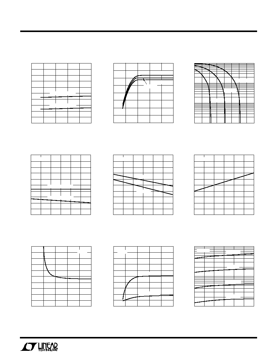
Supply Current
TYPICAL PERFOR
M
A
N
CE CHARACTERISTICS
U
W
INPUT VOLTAGE (V)
0
SUPPLY CURRENT (mA)
20
18
16
14
12
10
8
6
4
2
0
40
1161 G01
10
20
30
50
ALL CHANNELS ON
ALL CHANNELS OFF
Automatic Restart Period
INPUT VOLTAGE (V)
0
V
GATE
V
+
30
50
1161 G02
10
20
40
16
14
12
10
8
6
4
2
0
T
J
= 85°C
T
J
= 40°C
T
J
= 25°C
MOSFET Gate Voltage Above V
+
GATE VOLTAGE ABOVE V
+
(V)
0
2
4
8
GATE DRIVE CURRENT (
µ
A)
100
10
1
0.1
6
10
12
14
16
1161 G03
V
+
24V
V
+
= 8V
V
+
= 12V
MOSFET Gate Drive Current
TEMPERATURE (°C)
50
SUPPLY CURRENT (mA)
25
0
25
50
1161 G04
75
20
18
16
14
12
10
8
6
4
2
0
100
V
+
= 24V
ALL CHANNELS ON
ALL CHANNELS OFF
Supply Current
TEMPERATURE (°C)
50
INPUT THRESHOLD VOLTAGE (V)
25
0
25
50
1161 G05
75
2.4
2.2
2.0
1.8
1.6
1.4
1.2
1.0
0.8
0.6
0.4
100
V
+
= 24V
TURN-ON
TURN-OFF
Input Threshold Voltage
TEMPERATURE (°C)
50
DRAIN SENSE THRESHOLD VOLTAGE (mV)
25
0
25
50
1161 G06
75
110
100
90
80
70
60
50
40
30
20
10
100
V
+
= 24V
Drain Sense Threshold Voltage
INPUT VOLTAGE (V)
0
TURN-ON TIME (
µ
s)
500
450
400
350
300
250
200
150
100
50
0
40
1161 G07
10
20
30
50
IRFZ34
Turn-ON Time Driving MOSFET
INPUT VOLTAGE (V)
0
TURN-OFF TIME (
µ
s)
100
90
80
70
60
50
40
30
20
10
0
40
1161 G08
10
20
30
50
IRFZ34
NORMAL
CURRENT LIMIT
Turn-OFF Time Driving MOSFET
TEMPERATURE (°C)
50
10
RESTART PERIOD (ms)
100
1000
25
25
0
50
75
100
1161 G09
V
+
= 24V
C
T
= 3.3
µ
F
C
T
= 1
µ
F
C
T
= 0.33
µ
F
C
T
= 0.1
µ
F
4
LT1161
Supply Pins: The two supply pins are internally connected
and must also be externally connected. In addition to
providing the operating current for the LT1161, the supply
pins also serve as the Kelvin connection for the current
sense comparators. The supply pins must be connected to
the positive side of the drain sense resistors for proper
operation of the current sense.
Input Pins: The input pins are active high and each pin
activates a separate internal charge pump when switched
ON. The input threshold is TTL/CMOS compatible but may
be taken as high as 15V with or without the supply
powered. Each input has approximately 200mV of hyster-
esis and an internal 75k pull-down resistor.
Gate Pins: The gate pins drive the power MOSFET gates.
When an input is ON, the corresponding gate pin is
pumped approximately 12V above the supply. These pins
have a relatively high impedance when above the rail (the
equivalent of a few hundred kilohms). Care should be
taken to minimize any loading by parasitic resistance to
ground or supply.
Sense Pins: Each sense pin connects to the input of a
supply-referenced comparator with a 65mV nominal off-
set. When a sense pin is taken more than 65mV below
PI
N
FU
N
CTIO
N
S
U
U
U
supply, the MOSFET gate for that channel is driven low and
the corresponding timing capacitor discharged. Each cur-
rent-sense comparator operates completely independently.
The 65mV typical threshold has a +0.33%/
°
C temperature
coefficient, which closely matches the TC of drain sense
resistors formed from copper PC traces.
Some loads require high in-rush currents. An RC time
delay can be added between the drain sense resistor and
the sense pin to ensure that the current-sense comparator
does not false trigger during start-up (see Applications
Information). However, a maximum of 10k
can be in-
serted between a drain sense resistor and the sense pin. If
current sense is not required in any channel, the sense pin
for that channel is tied to supply.
Timer Pins: A timing capacitor C
T
from each timer pin to
ground sets the restart time following overcurrent detec-
tion. C
T
is rapidly discharged to less than 1V and then
recharged by a 14
µ
A nominal current source back to the
timer threshold, whereupon restart is attempted. If current
sense is not required in any channel, the timer pin for that
channel is left open.
Ground Pins: The two ground pins are internally con-
nected and must also be externally connected.
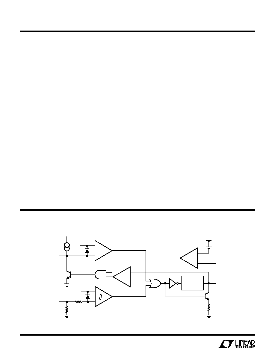
FU
N
CTIO
N
AL DIAGRA
U
U
W
+
+
+
+
OSCILLATOR
AND
CHARGE PUMP
1.4V
75k
75k
1.4V
3V
TIMER
14
µ
A
INPUT
65mV
V
+
SENSE
GATE
1161 FD
(Each Channel)
5
LT1161
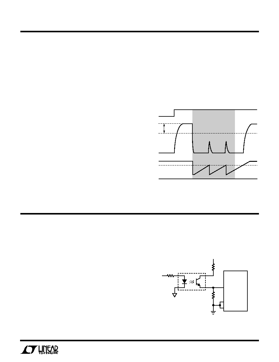
OPERATIO
U
When the MOSFET gate voltage is less than 1.4V, the timer
pin is released. The 14
µ
A current source then slowly
charges the timing capacitor back to 3V where the charge
pump again starts to drive the gate pin high. If a fault still
exists, such as a short circuit, the sense comparator
threshold will again be exceeded and the timer cycle will
repeat until the fault is removed (see Figure 2).
The LT1161 gate pin has two states, OFF and ON. In the
OFF state it is held low, while in the ON state it is pumped
to 12V above supply by a self-contained 750kHz charge
pump. The OFF state is activated when either the input pin
is below 1.4V or the timer pin is below 3V. Conversely, for
the ON state to be activated, both the input and timer pins
must be above their thresholds.
If left open, the input pin is held low by a 75k resistor, while
the timer pin is held a diode drop above 3V by a 14
µ
A pull-
up current source. Thus the timer pin automatically re-
verts to the ON state, subject to the input also being high.
The input has approximately 200mV of hysteresis.
The sense pin normally connects to the drain of the power
MOSFET, which returns through a low valued drain sense
resistor to supply. When the gate is ON and the MOSFET
drain current exceeds the level required to generate a
65mV drop across the drain sense resistor, the sense
comparator activates a pull-down NPN which rapidly pulls
the timer pin below 3V. This in turn causes the timer
comparator to override the input pin and activate the gate
pin OFF state, thus protecting the power MOSFET. In order
for the sense comparator to accurately sense MOSFET
drain current, the LT1161 supply pins must be connected
directly to the positive side of the drain sense resistors.
INPUT
1161 F02
OFF
NORMAL
OVERCURRENT
NORMAL
12V
V
+
GATE
0V
3V
0V
TIMER
Figure 2. Timing Diagram
APPLICATIO
N
S I
N
FOR
M
ATIO
N
W
U
U
U
Input/Supply Sequencing
There are no input/supply sequencing requirements for
the LT1161. The input may be taken up to 15V with the
supply at 0V. When the supply is turned on with an input
high, the MOSFET turn-on will be inhibited until the timing
capacitor charges to 3V (i.e., for one restart cycle). The
two V
+
pins (11, 20) must always be connected to each
other.
Isolating the Inputs
Operation in harsh environments may require isolation to
prevent ground transients from damaging control logic.
The LT1161 easily interfaces to low cost opto-isolators.
The network shown in Figure 3 ensures that the input will
be pulled above 2V, but not exceed the absolute maximum
LT1161
12V TO 48V
IN
GND
100k
1161 F03
2k
LOGIC
INPUT
1/4 NEC PS2501-4
LOGIC
GND
POWER
GROUND
51k
GND
(Each Channel, Refer to Functional Diagram)
Figure 3. Isolating the Inputs
rating, for supply voltages of 12V to 48V over the entire
temperature range. In order to maintain the OFF state, the
opto must have less than 20
µ
A of dark current (leakage)
hot.